Teledyne LeCroy Kibra DDR User Manual
Page 169
Kibra DDR Protocol Analyzer User Manual
167
DDR3 and DDR4 JEDEC Timing Violations Summary
Teledyne LeCroy
5.1.41
V42 - tMOD Mode Register Set Command to a Valid Command
Defines the interval between Mode Register Set and the next valid command. tMOD
violations can also occur during write leveling. This is calculated as max(12 nCK, 15ns) for
all speed bins.
5.1.42
V43 - tXPR First Clock Enable High after Reset to MRS
Defines the interval after initiating Reset (Clock Enable High) to normal operations. This is
defined as max(5nCK, tRFC(min) + 10ns) for all speed bins.
5.1.43
V44 - CCD-S Read to Read Delay (short) Different bank group, same rank
DDR4
Defined as the minimum interval between a READ command and another READ
command to a different bank group within the same Rank.
5.1.44
V45 - tWTW-DBGWrite to Write Delay (short) Different bank group; same
rank-DDR4
Defined as the minimum interval between a WRITE command and another WRITE
command to a different bank group within the same Rank. This is calculated as WL (AL +
CWL) + tWPRE + BL/2 + WTW‐S.
5.1.45
V46 - tWTR- DBGWrite to Read Delay (short) Different bank group; same
rank DDR4
Defined as the minimum interval between a WRITE command the next READ command to
a different bank group within the same Rank. This is calculated as WL (AL + CWL) +
tWPRE + BL/2 + WTR‐S
5.1.46
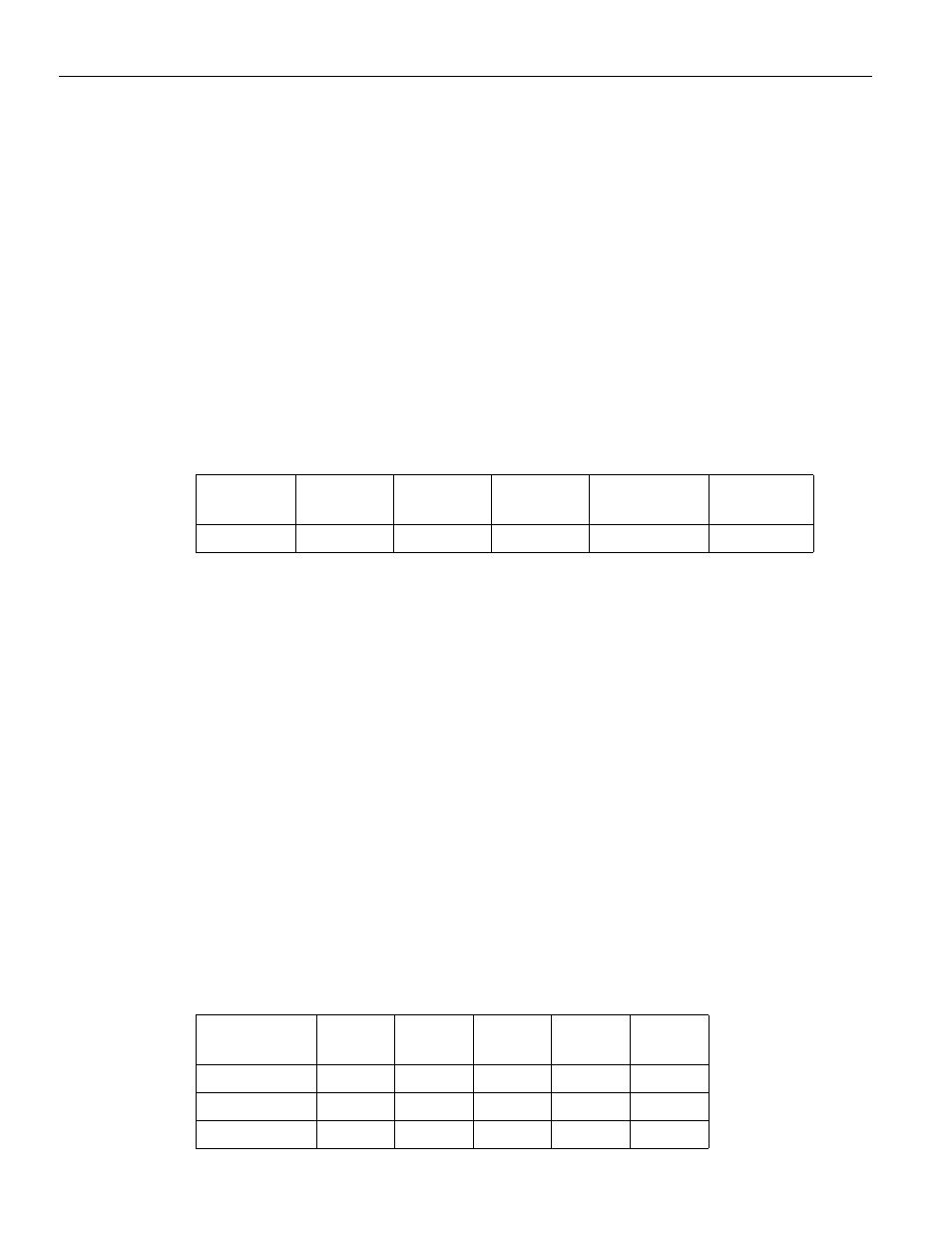
V47 - tRRD-SActivate to Activate Delay (short) Different bank group; same
rank DDR4
Defined as the minimum interval between an ACTIVATE command the next ACTIVATE
command to a different bank group within the same Rank.
Speed
Grade
1600
1866
2133
2400
3200
Min (nCK)
4
4
4
TBD
TBD
Speed Grade
1800
1866
2133
2400
3200
X4 Min (nCK)
4
4
4
4
4
X8
4
4
4
4
4
X16
5
5
5
6
7