Application note, 1 ddr3 and ddr4 jedec timing violations summary, Appendix a: application note – Teledyne LeCroy Kibra DDR User Manual
Page 161: Appendix a
Kibra DDR Protocol Analyzer User Manual
Appendix A
Application Note
5.1
DDR3 and DDR4 JEDEC Timing Violations Summary
This Application Note summarizes the JEDEC timing violations for DDR3 and DDR4
currently supported in Teledyne LeCroy’s Kibra 380 or Kibra 480 Protocol Analyzer. These
timing parameters are determined based on the CL, CWL, AL and operational timing mode
specified by the system memory controller and the SPD data in the DIMM.
5.1.1
V01 - tRAS ACTIVATE to PRECHARGE command period (Min)
The minimum interval between Activate and PreCharge is specified to ensure the active
row is closed before the next Activate or Refresh. This is the minimum amount of time
that must occur between activating a row and issuing a precharge to the row in same rank
and same bank. This makes sure that all the data from the row has been moved to the
sense amps and is stable before a precharge is issued to write the data back to the row.
5.1.2
V02 - tRAS ACTIVATE to PRECHARGE command period (Max)
The maximum interval between ACTIVATE and PRECHARGE to the same rank and same
bank is specified and is consistent with the Row to Row Delay (RRD). 9*tREFI is also the
maximum amount of time between refresh commands. As all Banks must be idle before
refresh, the maximum amount of time a Row can be active is the maximum amount of
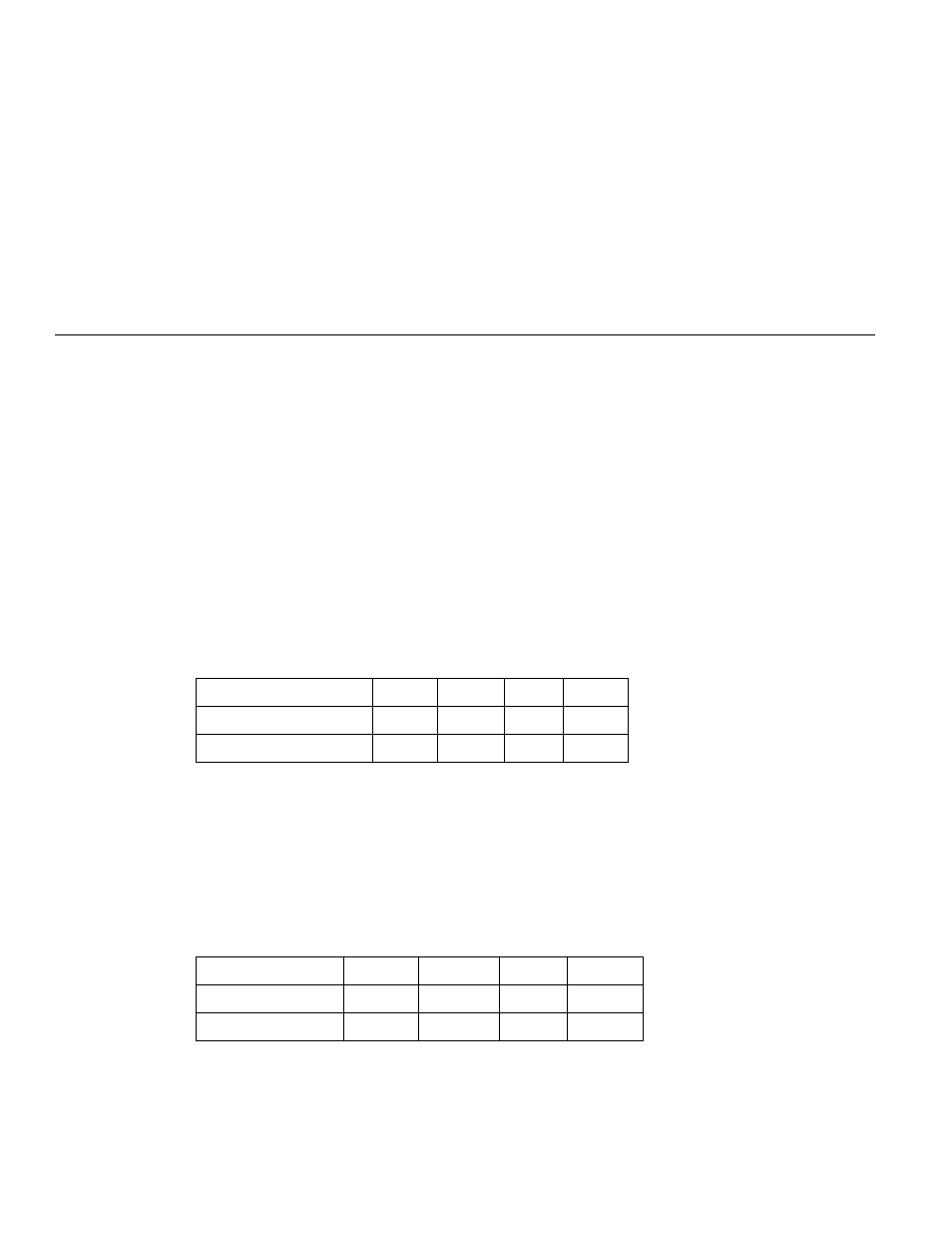
time between refresh commands. This table is for Tcase = [0‐85°C].
Speed Grade
800
1066
1333
1600
tRASmin (ns)
37.5
37.5
36
35
tRASmin (nCK)
15
20
24
28
Speed Grade
800
1066
1333
1600
tRASmax (ns)
70200
70200
70200
70200
tRASmax (nCK)
28080
37416
46823
56160