Teledyne LeCroy Kibra DDR User Manual
Kibra ddr protocol analyzer suite user manual
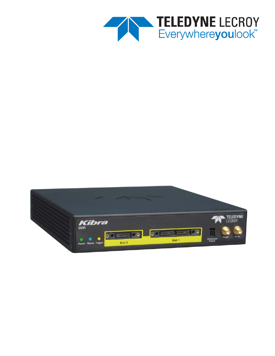
Table of contents
Document Outline
- Contents
- Introduction
- 1.1 Kibra 380 or Kibra 480 Overview
- 1.2 Specifications
- 1.3 Installing Your Kibra 380 or Kibra 480 Protocol Analyzer
- 1.4 Hardware Setup
- 1.5 DDR Interposer
- 1.6 CrossSync Control Panel
- 1.7 Launching Your Kibra 380 or Kibra 480 Software
- 1.8 Using the Software
- 1.9 Protocol Analyzer
- Protocol Analysis
- 2.1 Main Window
- 2.2 Software Menus and Toolbar
- 2.3 Application Menu Options
- 2.4 File
- 2.5 Setup
- 2.6 Recording Options Setup
- 2.7 Devices
- 2.8 CrossSync Control Panel
- 2.9 Preferences
- 2.10 Reset Interposers
- 2.11 Init Phy
- 2.12 Session
- 2.13 Analysis
- 2.14 Waveform View
- 2.15 Listing View
- 2.16 Bank State View
- 2.17 Traffic Summary
- 2.18 Timing Calculator View
- 2.19 Last MRS Values
- 2.20 Row Usage Report
- 2.21 Timing Violation Analysis
- 2.22 Trace Info
- 2.23 Navigation
- 2.24 View
- 2.25 Window
- 2.26 Help
- 2.27 Example Files
- Viewer Display
- 3.1 Window Management
- 3.2 Waveform View
- 3.2.1 Clock Position Selection
- 3.2.2 Data View Pane
- 3.2.3 Viewport Slider in Navigation Bar
- 3.2.4 Snap to Edge
- 3.2.5 Placing Cursors
- 3.2.6 Zoom In and Zoom Out
- 3.2.7 Overlay Signals Mode
- 3.2.8 Zoom Box
- 3.2.9 Signal Names Context Sensitive Menu
- 3.2.10 Context Sensitive Menu
- 3.2.11 Choosing Chip Select Color Highlighting
- 3.2.12 Timing and Protocol Violations
- 3.2.13 Right-Click Functionality in Waveform View
- Go to Next Gap
- Goes to the next gap (see See “Gap Markers” on page 131).
- Go to Previous Gap
- Go to Marker
- Go to Cursor
- Go to Trigger
- Go to Time
- Go to Selection
- Set New Marker
- Set and Edit New Marker
- Place Marker
- Edit This Marker
- Edit Marker
- Go to Next Transition [Alert]
- Go to Previous Transition [Alert]
- Delete This Marker
- Delete Marker
- Delete All Markers
- Add Lines
- Delete Line [Alert]
- Show/Hide Sub Signals
- Preferences
- 3.2.14 Markers
- 3.3 Viewport Slider/Navigation Bar
- 3.4 Listing View
- 3.5 Bank State View
- 3.6 Traffic Summary
- 3.7 Timing Calculator View
- 3.8 Last MRS Values
- 3.9 Row Usage Report
- 3.10 Timing Violation Reanalysis
- Real Time Statistics
- Application Note
- 5.1 DDR3 and DDR4 JEDEC Timing Violations Summary
- 5.1.1 V01 - tRAS ACTIVATE to PRECHARGE command period (Min)
- 5.1.2 V02 - tRAS ACTIVATE to PRECHARGE command period (Max)
- 5.1.3 V03 - tRRD ACTIVATE to ACTIVATE command period (DDR3 different bank, same rank) (DDR4 - same bank group)
- 5.1.4 V04 - tFAW Four Activate Window
- 5.1.5 V05 - tRCDx ACTIVATE to internal read or write delay (same bank)
- 5.1.6 V06 - tWTP WRITE to PRECHARGE delay
- 5.1.7 V07 - tRTPx READ to PRECHARGE delay
- 5.1.8 V08 - tRP PRECHARGE to a Valid Command
- 5.1.9 V09 - tWRA WRA to a Valid Command
- 5.1.10 V10 - t RFC REFRESH to a Valid Command
- 5.1.11 V11 - tREFI REFRESH Interval
- 5.1.12 V12 - tRTR READ to READ delay (DDR3 - same rank) (DDR4 - same bank group)
- 5.1.13 V13 - tdrRTR READ to READ delay (different rank - same DIMM)
- 5.1.14 V14 - tddRTR READ to READ delay (different DIMM)
- 5.1.15 V15 - tRTW READ to WRITE delay (same rank)
- 5.1.16 V16 - tdrRTW READ to WRITE delay (different rank, same DIMM)
- 5.1.17 V17 - tddRTW READ to WRITE delay (different DIMM)
- 5.1.18 V18 - tWTR WRITE to READ delay ( DDR3 - same rank) (DDR4 - same bank group)
- 5.1.19 V19 - tdrWTR WRITE to READ delay (different rank, same DIMM)
- 5.1.20 V20 - tddWTR WRITE to READ delay (different DIMM)
- 5.1.21 V21 - tWTW WRITE to WRITE delay ( DDR3 - same rank) (DDR4 - same bank group)
- 5.1.22 V22 - tddWTW WRITE to WRITE delay (different rank, same DIMM)
- 5.1.23 V23 - tddWTW WRITE to WRITE delay (different DIMM)
- 5.1.24 V24 - tXS SELF REFRESH EXIT to a Valid Command (without DLL)
- 5.1.25 V25 - tXSDLL SELF REFRESH EXIT to a Valid Command (with DLL)
- 5.1.26 V26 - tCKESR SELF REFRESH ENTRANCE to SELF REFRESH EXIT
- 5.1.27 V27 - tACTPDEN ACTIVE to POWER DOWN ENTRY
- 5.1.28 V28 - REFPDEN REFRESH to POWER DOWN ENTRY
- 5.1.29 V30 - tPRPDEN PRECHARGE / PRECHARGE ALL to POWER DOWN ENTRY
- 5.1.30 V31 - tRDPDEN READ / READ AUTO to POWER DOWN ENTRY
- 5.1.31 V32 - tWRPDEN WRITE to POWER DOWN ENTRY
- 5.1.32 V33 - tWRAPDEN WRITE AUTO to POWER DOWN ENTRY
- 5.1.33 V34 - tXP POWER DOWN EXIT to a Valid Command without DLL
- 5.1.34 V35 - tXPDLL POWER DOWN EXIT to a Valid Command with DLL - DDR3
- 5.1.35 V36 - tCKE Clock Enable minimum pulse width
- 5.1.36 V37 - tPD POWER DOWN ENTRY to POWER DOWN EXIT
- 5.1.37 V38 - tZQCS SHORT Calibration Sequence to a Valid Command
- 5.1.38 V39 - tZQOper ZQCL to a Valid Command
- 5.1.39 V40 - tZQinit First ZQCL after Reset to a Valid Command
- 5.1.40 V41 - tMRD MODE Register Set to Mode Register Set
- 5.1.41 V42 - tMOD Mode Register Set Command to a Valid Command
- 5.1.42 V43 - tXPR First Clock Enable High after Reset to MRS
- 5.1.43 V44 - CCD-S Read to Read Delay (short) Different bank group, same rank DDR4
- 5.1.44 V45 - tWTW-DBG Write to Write Delay (short) Different bank group; same rank -DDR4
- 5.1.45 V46 - tWTR- DBG Write to Read Delay (short) Different bank group; same rank DDR4
- 5.1.46 V47 - tRRD-S Activate to Activate Delay (short) Different bank group; same rank DDR4
- 5.1.47 V48 - tXS-FAST SRX to a Valid Command with DLL - DDR4
- 5.2 Supplemental Timing Information
- 5.1 DDR3 and DDR4 JEDEC Timing Violations Summary
- China Restriction of Hazardous Substances Table
- How to Contact Teledyne LeCroy
- Index