Lvds connector pinout (j6), 6 lvds c – Comtech EF Data SDM-2020 User Manual
Page 164
SDM-2020 Satellite Modulator
Revision 7
ASI/LVDS Data Interfaces MN/SDM2020M.IOM
13-8
13.1.6
LVDS C
ONNECTOR
P
INOUT
(J6)
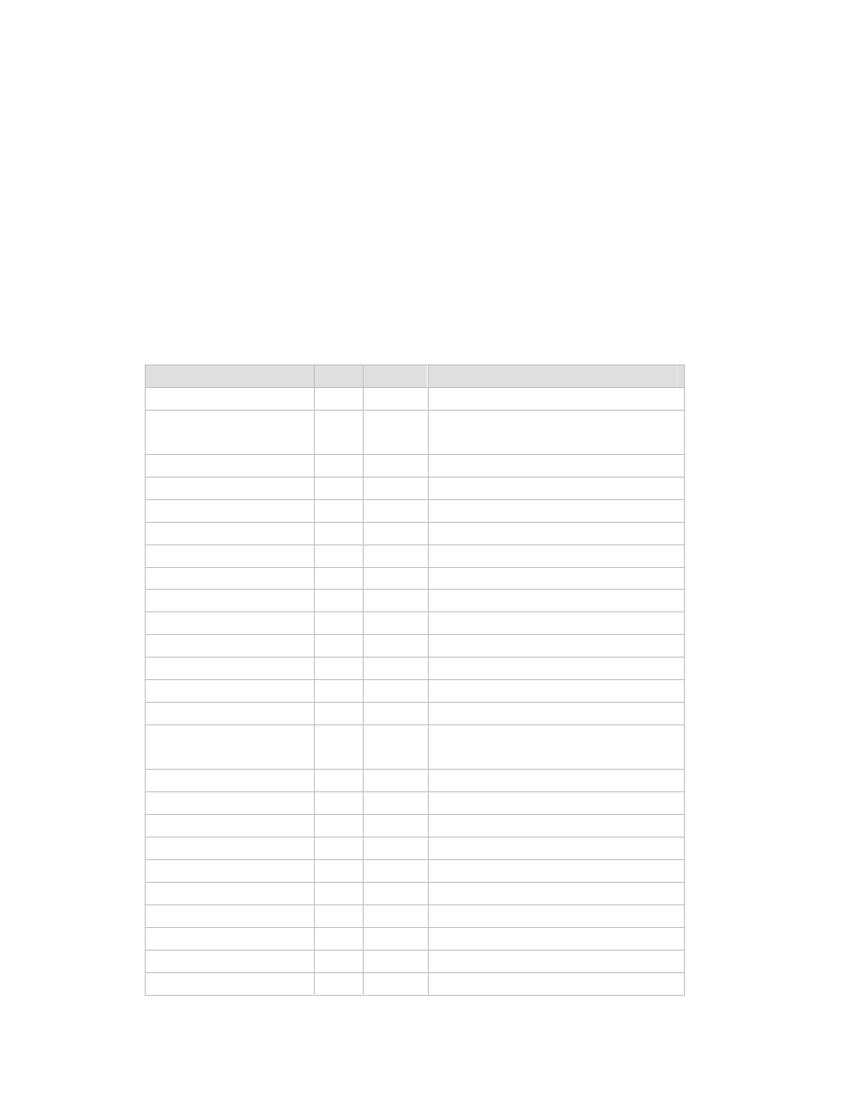
The LVDS connector is a 25-Pin D female type, with threaded jack nuts.
LVDS signal levels are as defined in EN50083-9. The differential sense of all signal pairs
is a logic “1” when “A” is positive with respect to “B.” Some DBS applications require
an inverted data or clock polarity and control of the signal polarity (normal or inverted) is
provided. Input/Output (I/O) of the interface is determined by:
• Whether it is plugged into a modulator or demodulator
•
Loopback or Loop Thru programming.
Signal Function/Name Pin #
Type
Comment
Clock A
1
I / O
Mod / Demod
System Gnd / REFCLKB
2
O / Gnd Mod / Demod
Demod – GND only, no clock available
Data 7 A(MSB/Serial)
3
I / O
Mod / Demod
Data 6 A
4
I / O
Mod / Demod
Data 5 A
5
I / O
Mod / Demod
Data 4 A
6
I / O
Mod / Demod
Data 3 A
7
I / O
Mod / Demod
Data 2 A
8
I / O
Mod / Demod
Data 1 A
9
I / O
Mod / Demod
Data 0 A
10
I / O
Mod / Demod
DVALID A
11
I / O
Mod / Demod
SYNC A
12
I / O
Mod / Demod
Cable Shield
13
I / O
Mod / Demod
Clock B
14
I / O
Mod / Demod
System Gnd / REFCLKA
15
O / Gnd Mod / Demod
Demod – GND 0nly, no clock available
Data 7 B
16
I / O
Mod / Demod
Data 6 B
17
I / O
Mod / Demod
Data 5 B
18
I / O
Mod / Demod
Data 4 B
19
I / O
Mod / Demod
Data 3 B
20
I / O
Mod / Demod
Data 2 B
21
I / O
Mod / Demod
Data 1 B
22
I / O
Mod / Demod
Data 0 B
23
I / O
Mod / Demod
DVALID B
24
I / O
Mod / Demod
SYNC B
25
I / O
Mod / Demod