Configuration, Onfiguration, Figure 8-1. lvds interface module pcb – Comtech EF Data SDM-2020 User Manual
Page 110
SDM-2020 Satellite Modulator
Revision 7
Low Voltage Differential Signal (LVDS)
MN/SDM2020M.IOM
8-3
Table 8-1. LVDS Specifications (Continued)
General Specifications
Signal Types
TX: TX Clock, TX Data, Data Valid, and Sync per TM1449.
The modulator does not require Sync or Data Valid with the 188 or 204 b
Voltage Levels
290 ± 40 mV differential into 100
Ω.
8.1.3
C
ONFIGURATION
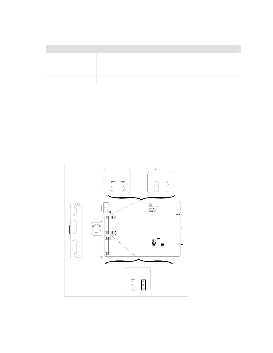
The interface provides DVB compliant operation when pins 2 and 15 are grounded using
the “DVB Configuration” jumper settings as described in the following paragraphs. A
reference clock from the modulator is output from the connector (J4) when the jumpers
are selected for SCT Output operation. See jumpers J1 and J6.
Note: SCT clock is always available on the Auxiliary Connector J5 and requires no
jumper settings.
In a demodulator, the LVDS interface (J3) only has provision for DVB Configuration,
and the Master Clock Input is not used. See jumpers J2 and J7.
J3
R
E
C
E
IV
E
O
U
T
J4
T
R
A
N
SM
IT
IN
J5
A
U
X
DEMODULATOR
DVB
CONFIGURATION
(FACTORY SETTING)
3
2
1
3
2
1
J2
J7
MODULATOR
DVB
CONFIGURATION
(FACTORY SETTING)
3
2
1
3
2
1
J1
J6
J4 - 2 & 15
SCT CLOCK OUTPUT
CLOCK
CONFIGURATION
J1
J6
3
2
1
3
2
1
J1 J6
J2 J7
Figure 8-1. LVDS Interface Module PCB