Comtech EF Data SDM-2020 User Manual
Page 113
SDM-2020 Satellite Modulator
Revision 7
Low Voltage Differential Signal (LVDS)
MN/SDM2020M.IOM
8-6
8.1.4.2
C
ONNECTOR
P
INOUTS
J4
The connector is a 25-pin sub-miniature D female, with threaded jack nuts for connector
pinout). All signals for this connector are inputs to the modulator, except the signal pair
on pins 2 and 15 (for an exception; see jumper settings). When used as a serial data port,
Data 7 (pins 3 and 16) are the active data pins. For DVB parallel operation Data 7
through Data 8 are used.
Signal levels are as defined in TIA/EIA-644. Per TM1449, the differential sense of all
signal pairs is a logic “1” when “A” is positive with respect to “B”. This is the normal
selection in the Configuration Interface menu. For DBS applications, the polarity of
signals may be inverted from the Configuration Interface menu.
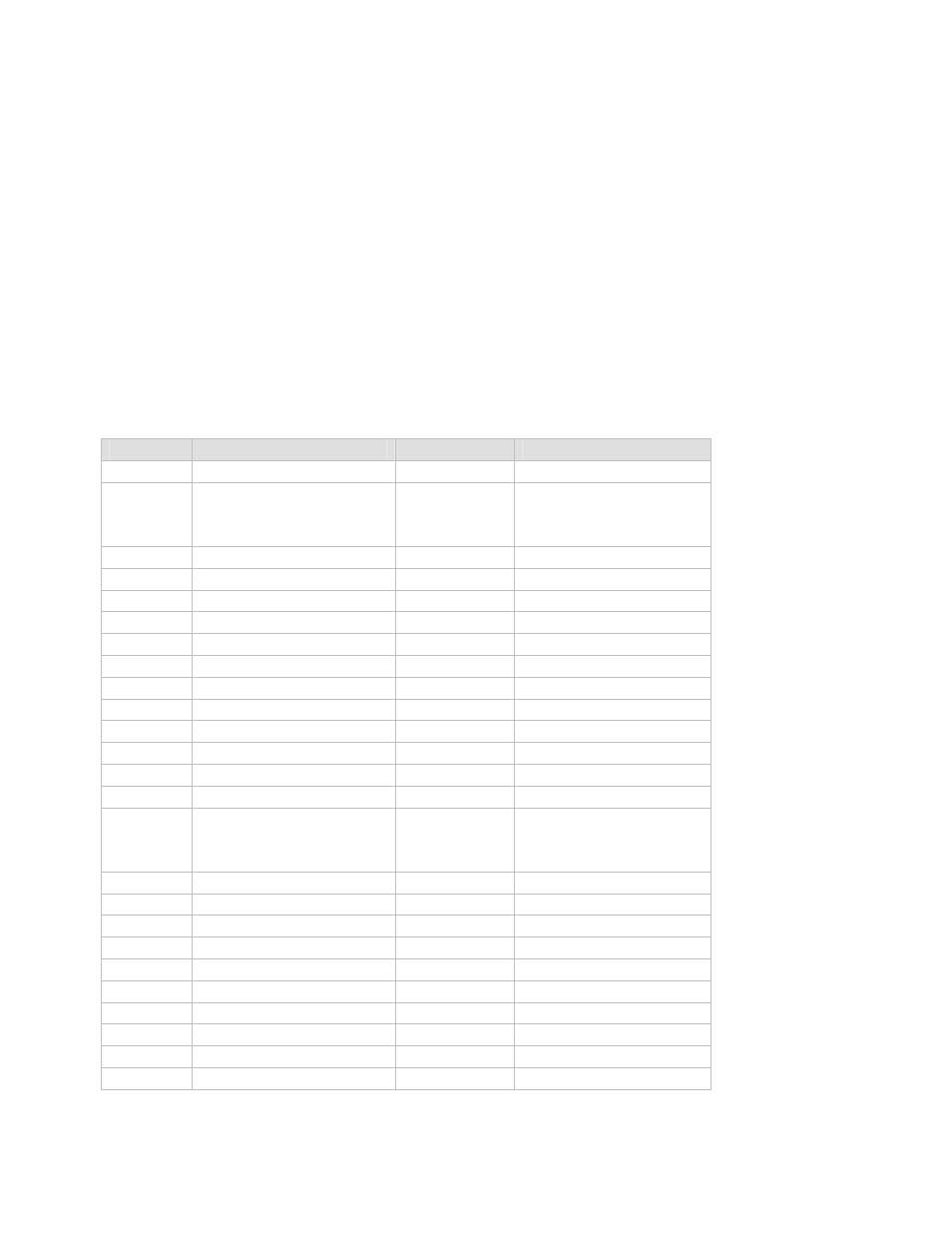
Table 8-3. DVB Interface Connector Pinout, J4 TX IN
Pin #
Signal Function/Name
Type
Comment
1 Clock
A
I
Mod
2 System
GND/REFCLKB
O/GND
Mod,
Jumper selectable
SCT output for Modulator
3
Data 7 A (MSB/Serial)
I
Mod
4
Data 6 A
I
Mod
5
Data 5 A
I
Mod
6
Data 4 A
I
Mod
7
Data 3 A
I
Mod
8
Data 2 A
I
Mod
9
Data 1 A
I
Mod
10
Data 0 A
I
Mod
11
DVALID A
I
Mod, Modulator Ignores
12 SYNC
A
I
Mod
13 Cable
Shield
I
Mod
14 Clock
B
I
Mod
15 System
GND/REFCLKA
O/GND Mod/Demod
Jumper selectable
SCT output for Modulator
16
Data 7 B (MSB/Serial)
I
Mod
17
Data 6 B
I
Mod
18
Data 5 B
I
Mod
19
Data 4 B
I
Mod
20
Data 3 B
I
Mod
21
Data 2 B
I
Mod
22
Data 1 B
I
Mod
23
Data 0 B
I
Mod
24 DVALID
B
I
Mod
25 SYNC
B
I
Mod