Configuration, Onfiguration – Comtech EF Data SDM-2020 User Manual
Page 102
SDM-2020 Satellite Modulator
Revision 7
RS-422 Data Interface
MN/SDM2020M.IOM
7-3
7.1.3
C
ONFIGURATION
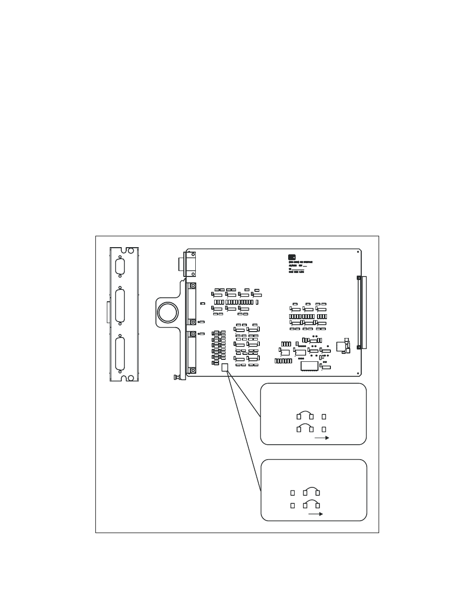
Note: The jumper location on the interface card and the optional positions are shown in
Figure
7-1.
A single jumper provides the option for a transmit or receive reference clock on
connector J3 (pins 2 and 15). The pins are configured at the factory as signal ground per
TM 1449. For Demodulator applications, where an SCT output is required in conjunction
with using the DVB Data port (J3). SCT may be jumped to pins 2 and 15, thus providing
all signals on a single connector.
The same jumper configuration in the demodulator applications provides for a Master
clock input. Alternatively, SCT and Master clock interconnects are available on the
Auxiliary port (J5).
D
OPTIONAL M2P CLOCK
CONFIGURATION FOR
MODULATOR ONLY
VB
CONFIGURATION
(FACTORY SETTING)
J3
D
V
B
P
ARALLE
L/
SERI
A
L
J4
E
IA
-53
0
SE
RIAL
J5
AUX
J
J
3
3
-
-
2
2
&
&
1
1
5
5
G
SCT CLOCK
OUTPUT
ND
NOTE:
JUMPER SELECTS FOR
PINS 2 & 15 OF THE J3
DVB PARALLEL/SERIAL
REAR PANEL CONNECTOR
Figure 7-1. RS-422 Interface Module PCB