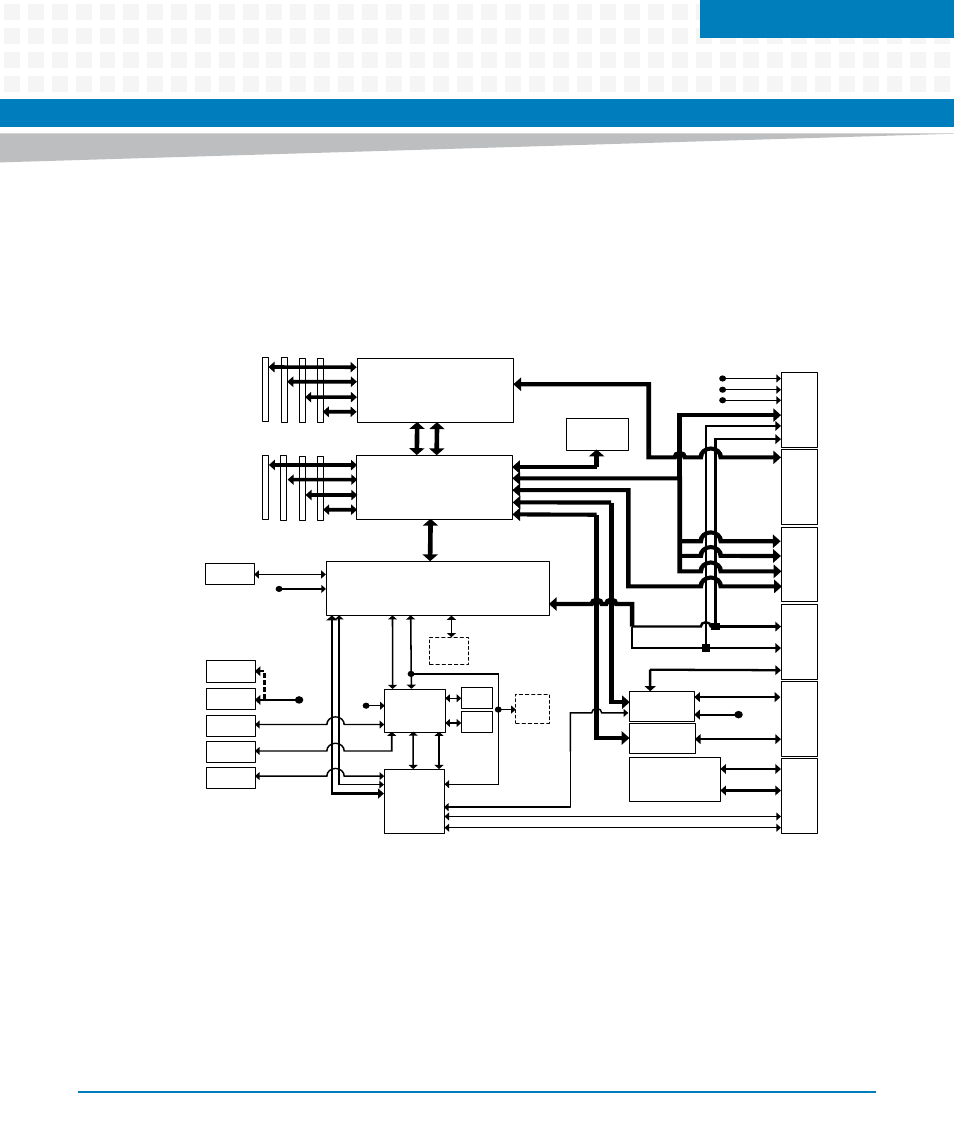
Functional description, 1 block diagram, Figure 5-1 – Artesyn ATCA 7370 / ATCA 7370-S Installation and Use (June 2014) User Manual
Page 105: Block diagram, Chapter 5
Chapter 5
ATCA-7370/ATCA-7370-S Installation and Use (6806800P54F)
105
Functional Description
5.1
Block Diagram
Note: On the single processor variant the second upper processor and its DIMM sockets are not
populated.
Figure 5-1
Block Diagram
Patsburg-B
PCH
82599
Dual 10GbE
Powerville
Quad GbE
Dual GbE-T (P2/3, Base)
FPGA
H8S
On-board Power
Supplies & Hot
Swap Circuitry
Zone1
to
Back
plane
P10
2x USB
Serial
Console
EFI
FW
EFI
FW
LPC
SPI
IPMB-A
IPMB-B
-48V
-48V
COM1
2x USB
SATA
QPI
Zone3
to
RTM
J30
Control, Power
COM2
COM2
1x USB
1x USB
SANDY BRIDGE-EP 0#
SANDY BRIDGE-EP 1#
TPM
DMI2
PCIe x8, Port3a,b
Reset
Button
Dual GbE-T (P0/1)
(optional)
PCIe x1
4x SAS 2.0
SPI
1000
Base-T
ATCA-7370-0GB
Zone3
to
RTM
J31
Zone3
to
RTM
J32
Zone2
to
Back
plane
J23
Zone2
to
Back
plane
J20
Dual 1/10GbE-X (Fabric)
2xUSB
SPI
4 DDR3 VLP DIMM Slots
4 DDR3 VLP DIMM Slots
SMB
SPI
PCIe x16 / Dual x8 / Quad x4, Port2a,b,c,d
2x SAS (UC1/2)
2x SAS
1000
Base-T
Dual GbE-T (P0/1)
PCIe x4
PCIe x4
PCIe x16
PCIe x4, Port1b
MO297
SSD
(optional)
(optional)
PCIe x4, Port1a
2x SAS (UC3/4)
PCIe x4
PCIe x4
PCIe x4
(optional)
2x SAS
Handle
Switch
1x GbE-X (P0, UC0)
PCIe x8 / Dual x4, Port3c,d
PCIe x16, Port2a,b,c,d
COM3
PCIe
Connector