Clock circuitry – Altera Cyclone II DSP Development Board User Manual
Page 67
Altera Corporation
Reference Manual
2–59
August 2006
Cyclone II DSP Development Board
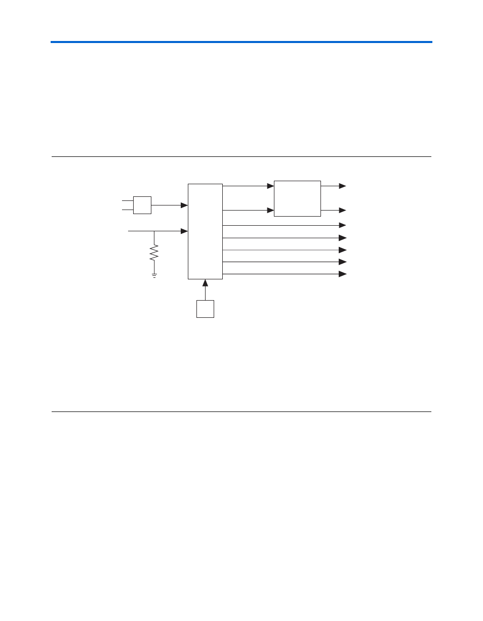
Cyclone II DSP Development Board Components
Clock Circuitry
This section describes the components used to set the Cyclone II DSP
development board clocking options.
shows the clock distribution on Cyclone II DSP development
board. The clocks must be defined first, this occurs within U16, the clock
buffer, which generates eight identical clock outputs (one output is
unconnected and two outputs are unused) used throughout the
Cyclone II DSP development board. See
.
Figure 2–21. Cyclone II DSP Development Board Clocking Options
Notes to
:
(1)
This signal is input to J35 as the FPGA clock (
FPGA_TO_DAC_CLK
). See
“D/A Converter Clocks” on page 2–18
.
(2)
This signal is input to J37 as the FPGA clock (
FPGA_TO_ADC_CLK
). See
“A/D Converter Clocks” on page 2–23
.
(3)
This signal is input to J23 as the PROTO clock (
PROTO_CLK_OSC
). See
.
(4)
This signal is input to J35 as the OSC clock (
CLK_OSC_DACA
“D/A Converter Clocks” on page 2–18
(5)
This signal is input to J37 as the OSC clock (
CLK_OSC_ADCA
“A/D Converter Clocks” on page 2–23
(6)
This signal is input to J34 as the OSC clock (
CLK_OSC_DACB
“D/A Converter Clocks” on page 2–18
(7)
This signal is input to J36 as the OSC clock (
CLK_OSC_ADCB
“A/D Converter Clocks” on page 2–23
CMOS
LVTTL
RT
PROTO OSC Clock Out (3)
DAC A Clock Out (4)
ADC A Clock Out (5)
On-Board Clock (U20)
Custom Clock (J20)
J19
SMA External Clock (J17)
J18
U12
EP2C35
FPGA Clock to DAC (1)
FPGA Clock to ADC (2)
CLKIN_TOP
CLKIN_BOT
U16
Clock
Buffer
DAC B Clock Out (6)
ADC B Clock Out (7)