Altera Cyclone II DSP Development Board User Manual
Page 13
Altera Corporation
Reference Manual
2–5
August 2006
Cyclone II DSP Development Board
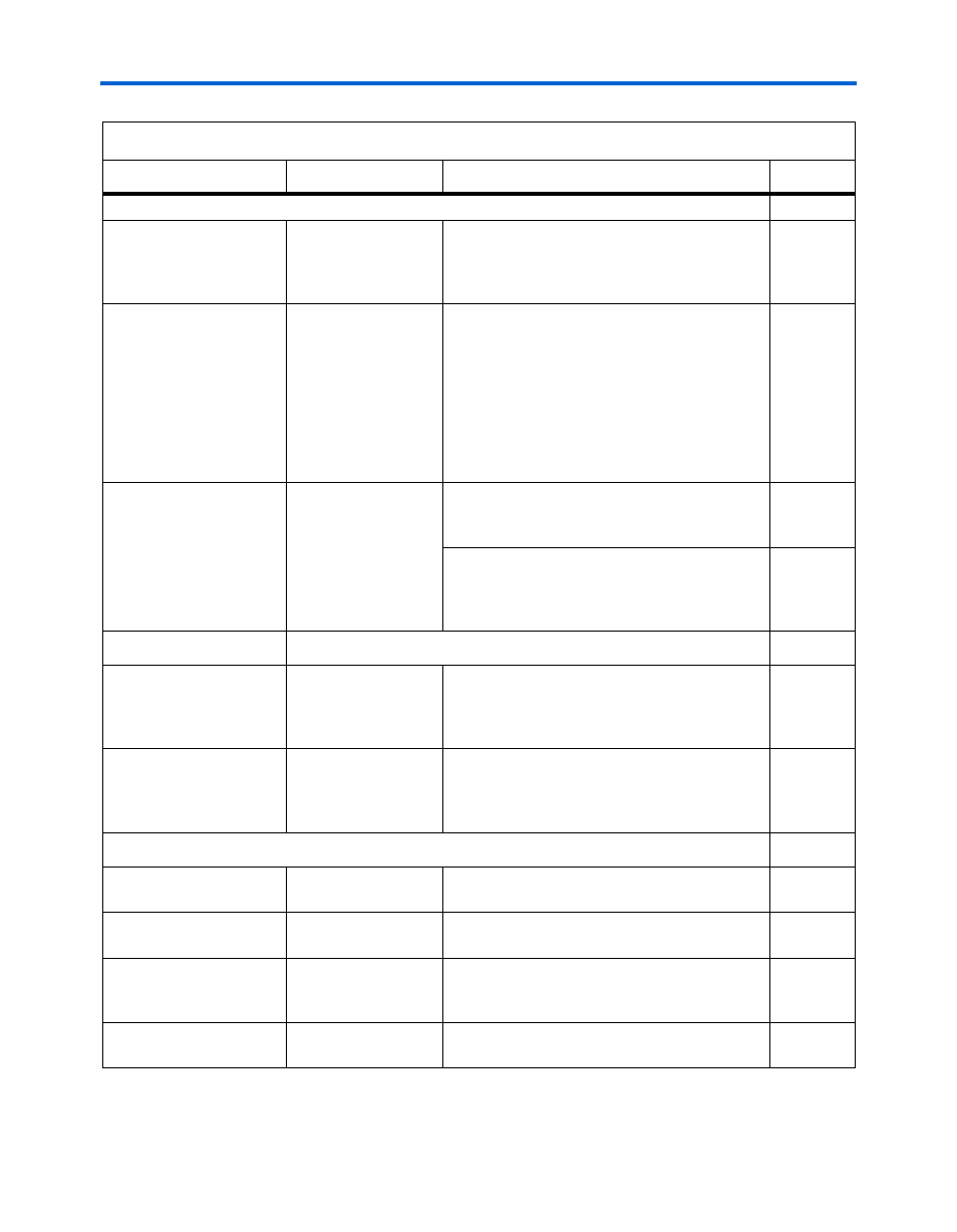
Cyclone II DSP Development Board Components
Memory Components
J8
Single slot connector
for DDR2 SDRAM
DIMM
Micron Technology MT8HTF3264AY-40E,
256 Mbyte, 32 Mbyte x 64, 167 MHz, 1.8 V,
240-pin, non-ECC, unbuffered DDR2 SDRAM
DIMM.
U17, U36
EPCS64 flash
memory
Two EPCS64 64 Mbit flash memory, serial
configuration devices used to store the safe
(factory) design (U17) and a user design (U36).
The EPCS64 device configures the EP2C70
FPGA by downloading the factory design or the
user design to the EP2C70 FPGA each time the
Cyclone II DSP development board powers up
or on board reset. J29 determines which design
is used.
U22
SSRAM
Cypress Semiconductor CY7C1360B-166AC,
9 Mbit, 256 Kbit x 36-bit/512 Kbit x 18 pipelined
synchronous SRAM (SSRAM).
The TMS320C6416 processor memory maps to
the Cyclone II DSP development board’s
SSRAM and the EP2C70 FPGA through the
EMIF connector (U34 and U40).
Expansion Connectors
J15, J22, J23
Expansion Prototype
Connector
Three connectors collectively called the
Expansion Prototype Connector. They are used
to connect to Altera daughter cards or for
debugging and prototyping purposes.
U34, U40
Expansion TI-EVM
connectors
Connects to the EMIF connector on the
TMS320C6416 DSK development board.
U34 and U40 are located on the back of the
Cyclone II DSP development board.
General Connectors
J9
JTAG connector
The Joint Test Action Group (JTAG) connector
is used to directly configure the EP2C70 FPGA.
J13
ASI connector
The active serial interface (ASI) connector is
used to program the EPCS64.
J12
Mictor connector
The Mictor connector used for hardware and
software debugging. It can be used with
external scopes or external logic analyzers.
J17
CLK SMA connector
SMA connector for an external clock input to
U16 to generate FPGA clocks.
Table 2–1. Cyclone II DSP Development Board Components & Interfaces (Part 2 of 5)
Board Reference
Name
Description
Page