Altera Cyclone II DSP Development Board User Manual
Page 14
2–6
Reference Manual
Altera Corporation
Cyclone II DSP Development Board
August 2006
Components & Interfaces
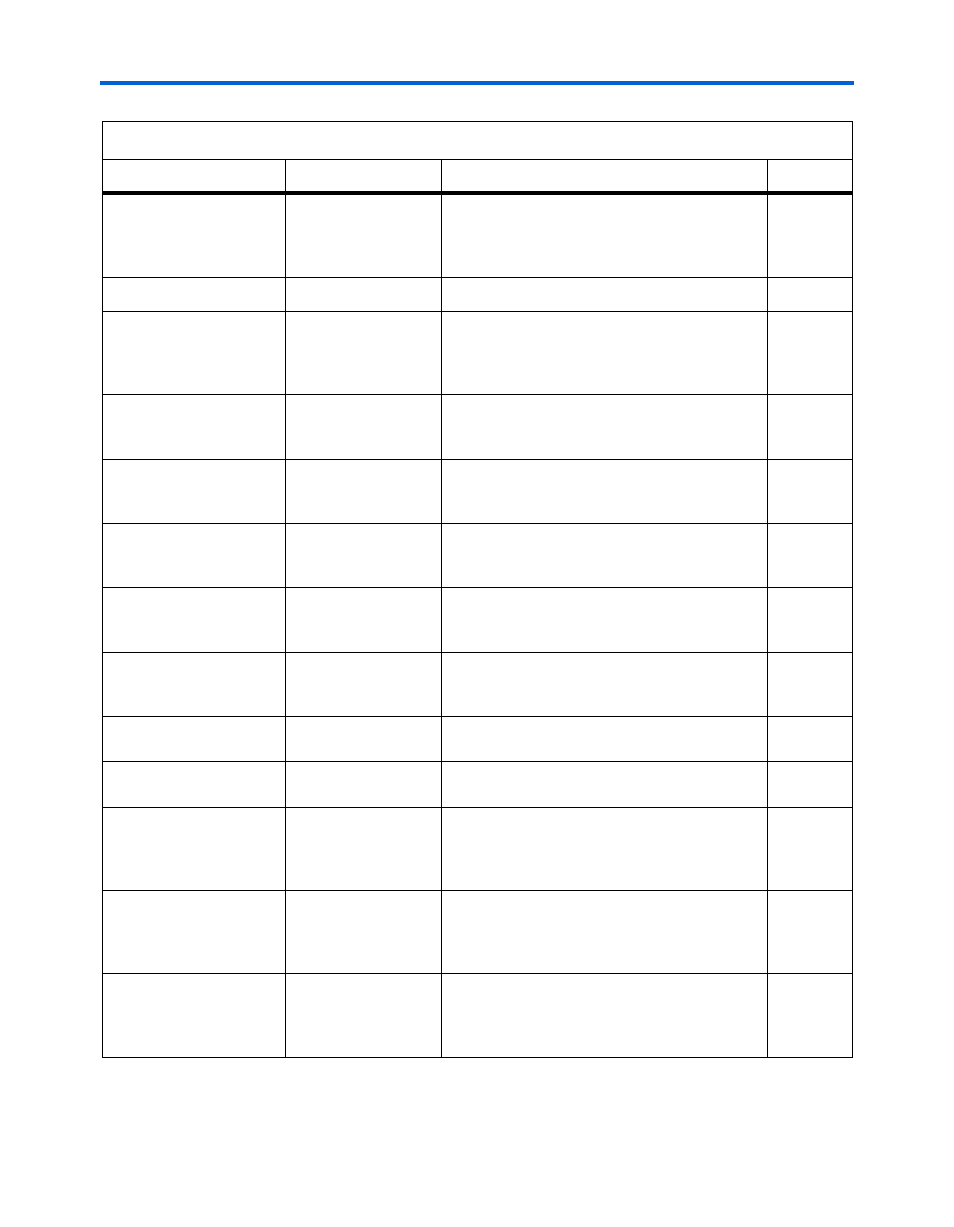
J11
DIMM_SYNC_CLK
SMA connector
The SMA connector (
DIMM_SYNC_CLK
) is a
test point SMA for eye diagrams of DDR2
signals using AC-coupled SMA connections to
an oscilloscope.
Jumpers
J18
On-board or custom
clock oscillator select
jumper
Jumper that determines if the on-board clock
100 MHz oscillator (U20) or a custom clock
oscillator (J20) becomes the input clock
oscillator to the clock buffer (U16).
J19
Clock select jumper
Jumper that determines which input to U16 (the
selected clock oscillator or the SMA clock) will
be used to determine the clock outputs of U16.
J24
SSRAM SLEEP
mode or RUN mode
jumper
Jumper that selects SLEEP mode or RUN mode
on the SSRAM.
J7
5 V enable/disable
jumper for U10
J7 disables the on-board 5-volt voltage
regulator (U10) output to eliminate all regulator-
based noise.
J25
D/A converter power
supply jumper
Jumper that selects whether the D/A converter
is powered from the DC input jack or the bench
power supply connector (J39 and J40).
J28
A/D converter power
supply jumper
Jumper that selects whether the A/D converter
is powered from the DC input jack or the bench
power supply connector (J42 and J41).
J33
D/A converter voltage
select jumper
Jumper that determines whether the D/A
converter is powered at 3.3 volts or 5.0 volts.
J29
EPCS select jumper
Jumper that selects the configuration mode
(SAFE EPCS or USER EPCS)
J30 (Channel A)
J38 (Channel B)
Data Format Select
(DFS) jumper
Data Format Select (DFS) jumper selects the
data output format from the Texas Instruments
ADS5520 A/D converter (U26 and U31). There
are four data output formats.
J35 (Channel A)
J34 (Channel B)
D/A converter clock
select jumper
D/A Converter Channel A clock select jumper. It
determines the D/A converter clock from three
input clock signals, the OSC clock, the FPGA
D/A converter clock, or the SMA clock (J26).
J37 (Channel A)
J36 (Channel B)
A/D converter clock
select jumper
A/D converter Channel A clock select jumper. It
determines the A/D converter clock from three
input clock signals, the OSC clock, the FPGA
A/D converter clock, or the SMA clock (J27).
Table 2–1. Cyclone II DSP Development Board Components & Interfaces (Part 3 of 5)
Board Reference
Name
Description
Page