D/a converter clocks – Altera Cyclone II DSP Development Board User Manual
Page 26
2–18
Reference Manual
Altera Corporation
Cyclone II DSP Development Board
August 2006
User Interfaces
lists the D/A converter reference for channels A and B.
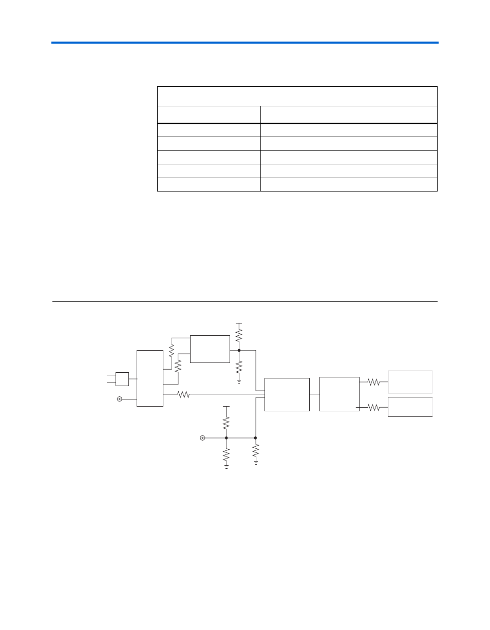
D/A Converter Clocks
shows the components involved in selecting the clock signal to
be sent to the TI DAC0904E (U25 for channel A, U30 for channel B). J35
(channel A) or J34 (channel B) selects the D/A clock from the OSC clock,
the FPGA clock, or the SMA clock (J26). The selected D/A clock passes
from J35 through a simple clock buffer (U27), which provides the clock
signal to the TI DAC904E.
Figure 2–7. TI DAC904E D/A Converter Clocking Options
Refer to
“Clock Circuitry” on page 2–59
for information on clock source selection.
Table 2–11. D/A Converter Reference (Channels A & B)
Item
Description
Board reference
U25 (channel A), U30 (channel B)
Part number
DAC904E
Device description
14-bit 165 MSPS D/A converter
Manufacturer
Texas Instruments
Manufacturer web site
www.ti.com
DAC External Clock SMA (J26)
50
143
95.3
143
95.3
33
33
J35 (Channel A)
or J34 (Channel B)
DAC Clock
Select
U27
DAC Clock
Buffer
U25 (Channel A)
TI DAC904E
U12
EP2C35
U16
Clock
Buffer
FPGA_TO_DAC_CLK
SMA_TO_DAC_CLK
CLK_OSC_DACA
External Clock SMA (J17)
On-Board Clock (U20)
Custom Clock (J20)
J18
CLKIN_TOP
CLKIN_BOT
33
33
33
U30 (Channel B)
TI DAC904E