Featured device, User interfaces, User interfaces –9 – Altera Cyclone II DSP Development Board User Manual
Page 17
Altera Corporation
Reference Manual
2–9
August 2006
Cyclone II DSP Development Board
Cyclone II DSP Development Board Components
Featured Device
The DSP Development Kit, Cyclone II Edition features the EP2C70F672
FPGA (U12) in a 672-pin FineLine BGA
®
lists the
“Power Switch (SW1)” on page 2–57
features of this device.
You can configure the FPGA in one of two ways:
■
Use Quartus II to program a SRAM Object file (SOF) file directly into
the FPGA via the JTAG connector.
f
For details about configuring the EP2C70 FPGA, see the Getting Started
chapter in the DSP Development Kit, Cyclone II Edition Getting Started User
Guide.
■
Use Quartus II to load a design into the EPCS64 device via the ASI
connector and then cycle power to load the design from the EPCS64
device into the FPGA.
There are two EPCS64 devices, J29 determines which EPCS64 device
loads the FPGA. Refer to
“EPCS64 Flash Memory Devices (U17,
for more information.
User Interfaces
This section describes the user interfaces, which consist of LEDs,
switches, push-buttons, seven-segment display, line in, line out, audio
and headphone jacks, VGA, D/A converter, and A/D converter.
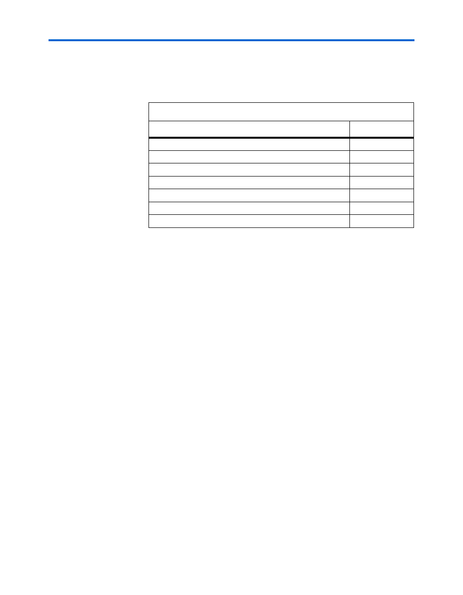
Table 2–2. Cyclone II EP2C70F672 Features
Feature
Value
Embedded 18x18 multipliers
150
Logic Elements (LEs)
68,416
M4K RAM blocks (4 Kbits + 512 parity bits)
250
Maximum differential channels
262
PLLs
4 PLLs
Total RAM bits
1,152,000
User I/O pins
422