Read dma example – Altera V-Series Avalon-MM DMA User Manual
Page 91

Address
Offset
Register Name
Description
0x04
WR_RC_HIGH_SRC_ADDR
Upper dword of the write DMA source address.
Specifies the address in the Avalon-MM domain from
which the Write DMA fetches data.
0x08
WR_CTLR_LOW_DEST_ADDR
Lower dword of the write DMA destination address.
Specifies the address in Root Complex memory to which
the Write DMA writes data.
0x0C
WR_CTRL_HIGH_DEST_ADDR
Upper dword of the write DMA destination address.
Specifies the address in Root Complex memory to which
the Write DMA writes data.
0x10
CONTROL
Specifies the following information:
• [31:25]: Reserved must be 0.
• [24:18]:
ID
: Specifies the
Descriptor ID
.
Descriptor
ID
0 is at the beginning of the table.
Descriptor ID
is at the end of the table.
• [17:0] :
SIZE
: The transfer size in dwords. Must be
non-zero. The maximum transfer size in 1 MBytes -
4 bytes.
0x14 -
0x1C
Reserved
N/A
Read DMA Example
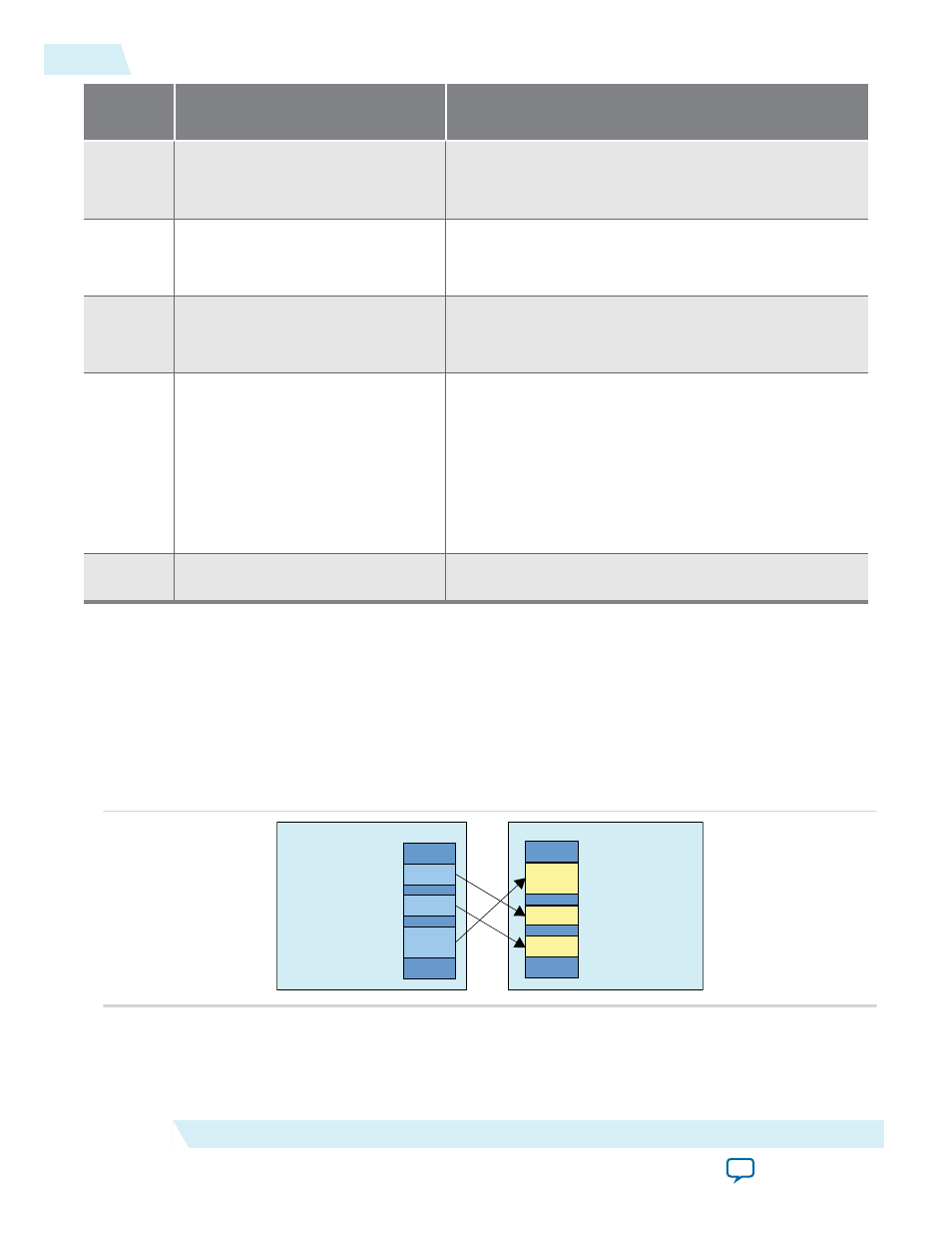
The following example moves three data blocks from the PCIe address space to the Avalon-MM address
space. Host software running on an embedded CPU allocates the memory and programs creates the
descriptor table in PCIe address space. The following figures illustrate the location and size of the data
blocks in the PCIe and Avalon-MM address spaces and the descriptor table format. In this example, the
value of
RD_TABLE_SIZE
is 127.
Figure 5-10: Data Blocks to Transfer from PCIe to Avalon-MM Address Space Using Read DMA
256 KB
512 KB
1 MB
Addr 0x1_2000_0000
Addr 0x2000_0000
Addr 0x1000_0000
PCIe System Memory
1 MB
256 KB
512 KB
Addr 0x5000_0000
Addr 0x1000_0000
Addr 0x0001_0000
Avalon-MM Memory
5-22
Read DMA Example
UG-01154
2014.12.18
Altera Corporation
Registers
