Pld_clk, Clock summary – Altera V-Series Avalon-MM DMA User Manual
Page 106
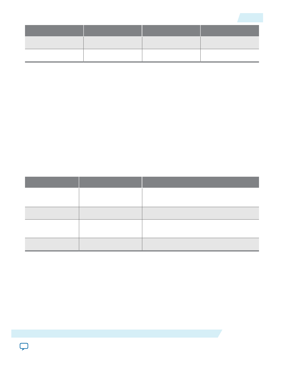
Link Width
Max Link Rate
Avalon Interface Width
coreclkout_hip
×4
Gen3
256
125 MHz
×8
Gen3
256
250 MHz
pld_clk
coreclkout_hip
can drive the Application Layer clock along with the
pld_clk
input to the IP core. The
pld_clk
can optionally be sourced by a different clock than
coreclkout_hip
. The
pld_clk
minimum
frequency cannot be lower than the
coreclkout_hip
frequency. Based on specific Application Layer
constraints, a PLL can be used to derive the desired frequency.
Note: For Gen3, Altera recommends using a common reference clock (0 ppm) because when using
separate reference clocks (non 0 ppm), the PCS occasionally must insert SKP symbols, potentially
causing the PCIe link to go to recovery. Gen1 or Gen2 modes are not affected by this issue. Systems
using the common reference clock (0 ppm) are not affected by this issue. The primary repercussion
of this issue is a slight decrease in bandwidth. On Gen3 x8 systems, this bandwidth impact is
negligible. If non 0 ppm mode is required, so that separate reference clocks are used, please contact
Altera for further information and guidance.
Clock Summary
Table 6-4: Clock Summary
Name
Frequency
Clock Domain
coreclkout_hip
62.5, 125 or 250 MHz
Avalon-ST interface between the Transaction and
Application Layers.
pld_clk
125 or 250 MHz
Application and Transaction Layers.
refclk
100 or 125 MHz
SERDES (transceiver). Dedicated free running input
clock to the SERDES block.
reconfig_xcvr_clk
100 –125 MHz
Transceiver Reconfiguration Controller.
UG-01154
2014.12.18
pld_clk
6-7
Reset and Clocks
Altera Corporation