5 memory read, 4 initial reset, 1 initial reset sequence – Epson S1C63000 User Manual
Page 31

S1C63000 CORE CPU MANUAL
EPSON
25
CHAPTER 3: CPU OPERATION
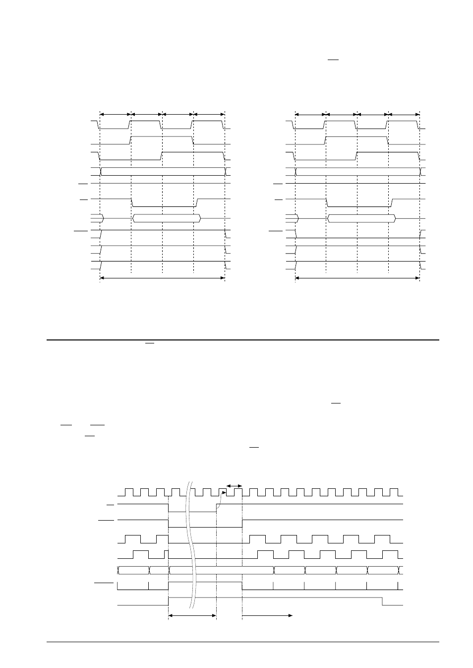
3.3.5 Memory read
In an execution cycle that reads data from the data memory, the read signal RD is output between the T2
and T3 states and data is read from the data bus. The address bus outputs the target address during this
bus cycle.
The 4-bit/16-bit access is the same as the memory write.
Fig. 3.4.1.1 Initial reset status and sequence after releasing
CLK
SR
STOP
PK
PL
PC
FETCH
Interrupt mask
Reset status
Sequence after releasing
ANY
ANY
ANY
ANY
110H
1 clock
LDB %BA,imm8 LDB %SP1,%BA LDB %BA,imm8 LDB %SP2,%BA
ANY
Interrupt mask
111H
112H
113H
114H
CLK
PK
PL
DA00–DA15
WR
RD
D0–D3
BS16
DBS1
DBS0
T1
T2
T3
T4
Bus cycle
Address
Read data
CLK
PK
PL
DA00–DA15
WR
RD
M00–M15
BS16
DBS1
DBS0
T1
T2
T3
T4
Bus cycle
Address
Read data
(a) During 4-bit data access
(b) During 16-bit data access
Fig. 3.3.5.1 Bus cycle during memory read
3.4 Initial Reset
The S1C63000 has a reset (SR) terminal in order to start the program after initializing the circuit when the
power is turned on or other situations. The following explains the operation at an initial reset and the
initial setting of the internal registers.
3.4.1 Initial reset sequence
The S1C63000 enters into an initial reset status immediately after setting the SR terminal to a low level,
and the internal circuits are initialized. During an initial reset, the data bus goes to a high-impedance and
the RD and WR signals go to a high level.
When the SR terminal goes to a high level, the initial reset is released and the program starts executing
from address 0110H. The release of an initial reset (the SR terminal goes a high level) is accepted at the
rising edge of the CPU operation clock (CLK), and the first bus cycle ( fetching the instruction of the
address 0110H) starts from 1 clock after.
