3 interrupt vector read, 4 memory write – Epson S1C63000 User Manual
Page 30

24
EPSON
S1C63000 CORE CPU MANUAL
CHAPTER 3: CPU OPERATION
3.3.3 Interrupt vector read
When an interrupt is generated, the CPU reads the interrupt vector output to the data bus by the periph-
eral circuit that has generated the interrupt. The interrupt vector read status indicates this bus cycle. The
peripheral circuit outputs the interrupt vector to the data bus during this status, and the CPU reads the
data between the T2 and T3 states. At this time, the CPU outputs the RDIV signal (for exclusive use of the
interrupt vector read) as a read signal, not the RD signal that is used for normal data memory read. The
address bus outputs a dummy address during this bus cycle. See Section 3.5 for the operation when an
interrupt is generated.
CLK
PK
PL
DA00–DA15
RDIV
WR
RD
D0–D3
DBS1
DBS0
T1
T2
T3
T4
Bus cycle
Dummy address
Interrupt vector
CLaK
PK
PL
DA00–DA15
WR
RD
D0–D3
BS16
DBS1
DBS0
T1
T2
T3
T4
Bus cycle
Address
Write data
(a) During 4-bit data access
(b) During 16-bit data access
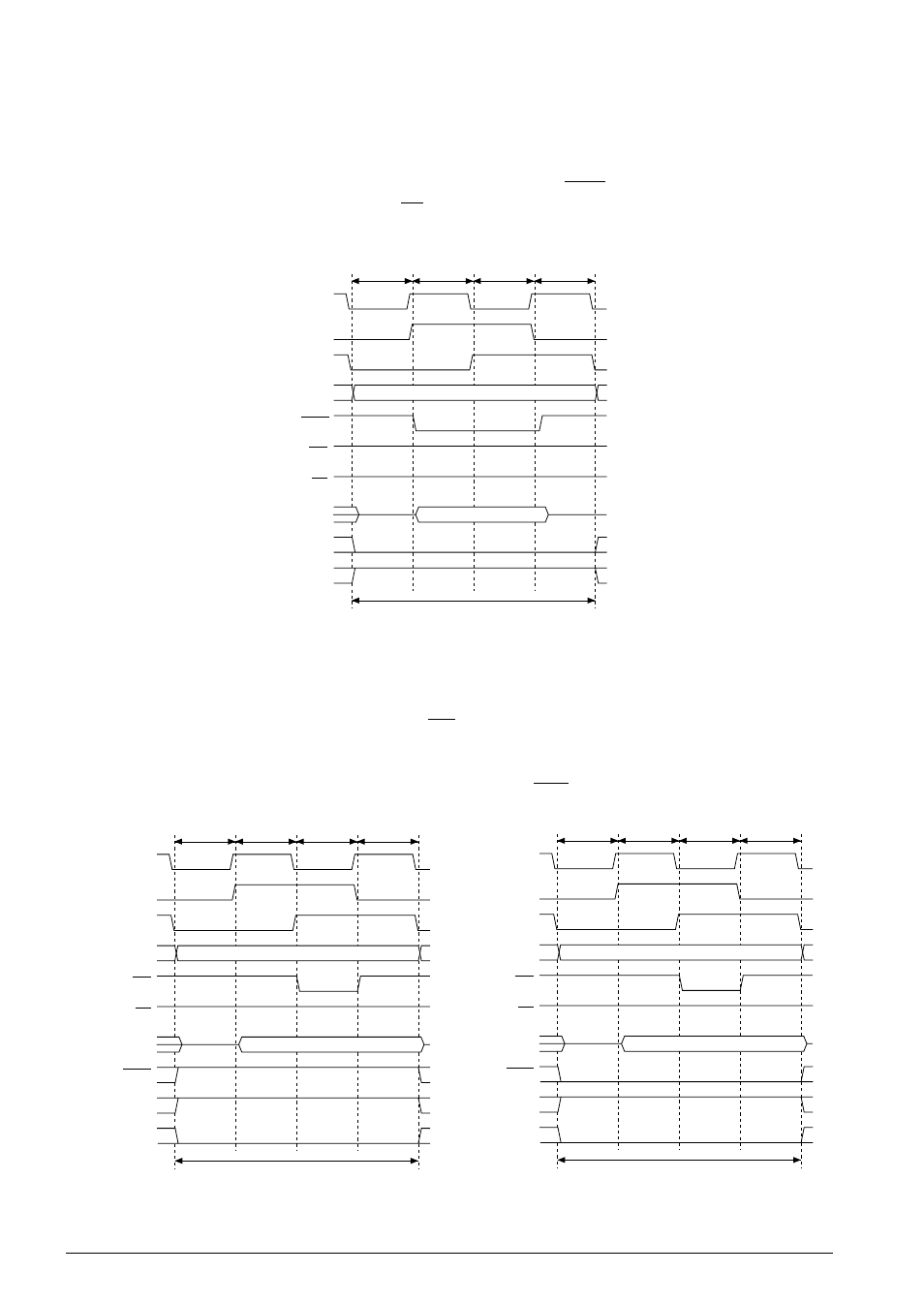
Fig. 3.3.4.1 Bus cycle during memory write
Fig. 3.3.3.1 Bus cycle during reading interrupt vector
3.3.4 Memory write
In an execution cycle that writes data to the data memory, the writing data is output to the data bus
between the T2 and T4 states and the write signal WR is output in the T3 state. The address bus outputs
the target address during this bus cycle.
The S1C63000 contains a 4-bit data bus (D0–D3) and a 16-bit data bus (M00–M15) for an address stacking.
The CPU switches the data bus according to the instruction. The BS16 signal is provided for this switch-
ing.
CLK
PK
PL
DA00–DA15
WR
RD
M00–M15
BS16
DBS1
DBS0
T1
T2
T3
T4
Bus cycle
Address
Write data
