Table 2-20 – Digilent 6003-410-000P-KIT User Manual
Page 66
66
XUP Virtex-II Pro Development System
UG069 (v1.0) March 8, 2005
Chapter 2: Using the System
R
configuration, start configuration, select the source of configuration, control the bitstream
revision, and reset the device.
For the System ACE controller to be properly synchronized with the MPU, the clocks must
be synchronized. The clock traces on the XUP Virtex-II Pro Development System that drive
the System ACE controller and the MPU interface sections of are matched in length to
maintain the required timing relationship.
The System ACE controller has very specific requirements for the way the file system is
created on the CompactFlash device. The FAT file system processing code cannot handle
more than one ROOT directory sector, 512 bytes, or 16 32-bit file/directory entries. If the
ROOT directory has more than 16 file/directory entries (including deleted entries), the
System ACE controller does not function properly. In addition, the System ACE controller
cannot handle CompactFlash devices whose FAT file system is set up with 1 cluster = 1
sector = 512 bytes.
The CompactFlash device must be formatted so that 1 cluster > 512 bytes, and the boot
parameter block must be setup with only 1 reserved sector. It is typical of newer operating
systems to format CompactFlash devices with more that 1 reserved sector.
The workaround for these System ACE controller requirements is to format the card with
a utility such as mkdosfs found at
The following command line produces the correct format on drive X: with a volume name
of XLXN_XUP.
C:\> mkdosfs –v –F 16 -R 1 –s 2 –n XLNX_XUP X:
(for a 16 MB CF card)
C:\> mkdosfs –v –F 16 -R 1 –s 8 –n XLNX_XUP X:
(for a 128 MB CF card)
C:\> mkdosfs –v –F 16 -R 1 –s 16 –n XLNX_XUP X:
(for a 512 MB CF card)
C:\> mkdosfs –v –F 16 -R 1 –s 64 –n XLNX_XUP X:
(for a 1 GB microdrive)
For more information on the System ACE MPU interface, consult the System ACE
CompactFlash Solution (
) data sheet.
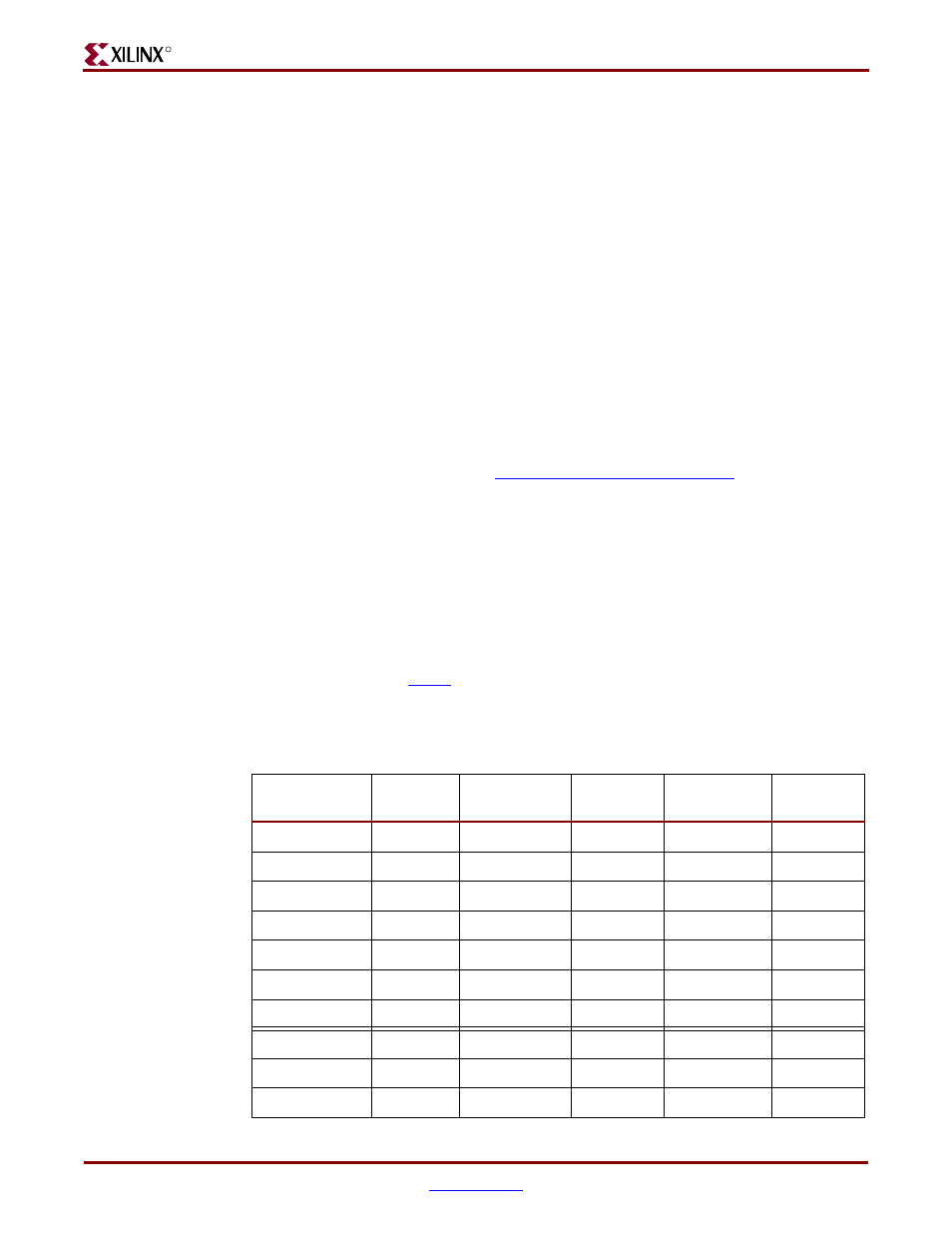
outlines the MPU interface connections between the FPGA and the System ACE
controller.
Table 2-20:
System ACE Connections
Signal
Direction
System ACE
Pin
FPGA Pin
I/O Type
Drive
CF_MPA[0]
O
70
AF21
LVCMOS25
8 mA
CF_MPA[1]
O
69
AG21
LVCMOS25
8 mA
CF_MPA[2]
O
68
AC19
LVCMOS25
8 mA
CF_MPA[3]
O
67
AD19
LVCMOS25
8 mA
CF_MPA[4]
O
45
AE22
LVCMOS25
8 mA
CF_MPA[5]
O
44
AE21
LVCMOS25
8 mA
CF_MPA[6]
O
46
AH22
LVCMOS25
8 mA
CF_MPD[0]
I/O
66
AE15
LVCMOS25
8 mA
CF_MPD[1]
I/O
65
AD15
LVCMOS25
8 mA
CF_MPD[2]
I/O
63
AG14
LVCMOS25
8 mA