Using the system, Configuring the power supplies, Chapter 2: using the system – Digilent 6003-410-000P-KIT User Manual
Page 19: Figure 2-1, Chapter 2
XUP Virtex-II Pro Development System
19
UG069 (v1.0) March 8, 2005
R
Chapter 2
Using the System
Configuring the Power Supplies
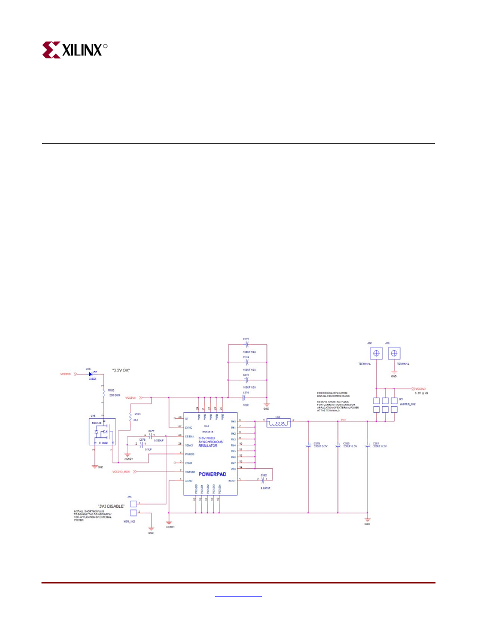
The XUP Virtex-II Pro Development System supports the independent creation of the
power supplies for the core voltage of 1.5V (FPGA_VINT), 2.5V general-purpose power,
I/O and/or VCCAUX supplies (VCC2V5), and 3.3V I/O and general-purpose power
(VCC3V3). These voltages are created by synchronous buck-switching regulators derived
from the 4.5V-5.5V power input provided at the center-positive barrel-jack power input
(J26) or the terminal block pair (J34-J35). Each of these supplies can be disabled through the
insertion of jumpers (JP2, JP4, and JP6), and the external application of power from the
terminal blocks (J28-J33). If external power is supplied, the associated internal power
supply must be disabled (through the insertion of JP6, JP2, or JP4) and the associated on-
board power delivery jumpers (JP5, JP1, or JP3) must be removed. The power consumption
from each of the on-board power supplies can be monitored through the removal of JP5,
JP1, or JP3 and the insertion of a current monitor. If any of the power supplies are outside
the recommended tolerance, internally or externally provided, the system enters a RESET
state indicated by the illumination of the RESET_PS_ERROR LED (D6) and the assertion of
the RESET_Z signal. A typical switching power supply is shown in
.
Figure 2-1:
Typical Switching Power Supply
ug069_04_021505