General description, Block diagram, Board components – Digilent 6003-410-000P-KIT User Manual
Page 14: Block diagram board components, Figure 1-1, Virtex-ii pro fpga
14
XUP Virtex-II Pro Development System
UG069 (v1.0) March 8, 2005
Chapter 1: XUP Virtex-II Pro Development System
R
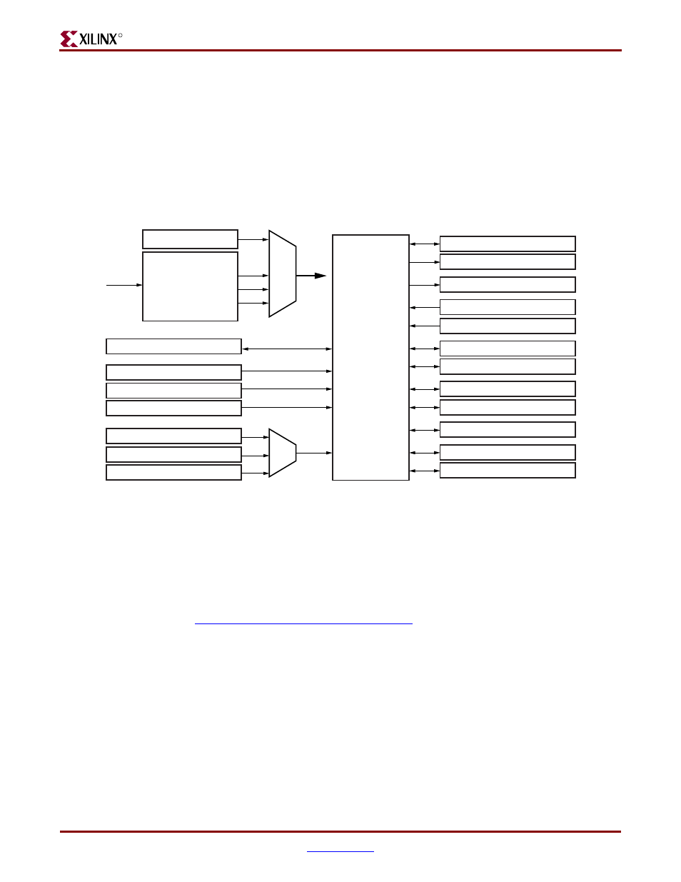
General Description
The XUP Virtex-II Pro Development System provides an advanced hardware platform that
consists of a high performance Virtex-II Pro Platform FPGA surrounded by a
comprehensive collection of peripheral components that can be used to create a complex
system and to demonstrate the capability of the Virtex-II Pro Platform FPGA.
Block Diagram
shows a block diagram of the XUP Virtex-II Pro Development System.
Board Components
This section contains a concise overview of several important components on the XUP
Virtex-II Pro Development System (see
). The most recent documentation for the
system can be obtained from the XUP Virtex-II Pro Development System support website
http://www.xilinx.com/univ/xup2vp.html
Figure 1-1:
XUP Virtex-II Pro Development System Block Diagram
CPU Debug Port
100 MHz System Clock
75 MHz SATA Clock
User Clocks (2)
Platform Flash Configurations (2)
Compact Flash Configurations (8)
USB2 High Speed Configuration
Internal Power Supplies
3.3V
2.5V
1.5V
External Power
4.5-5.5V
High Speed Expansion Port
5V Tolerant Expansion Headers
2 GB DDR SDRAM DIMM Module
Multi-Gigabit Transceiver Port
Serial ATA Ports (3)
RS-232 & PS/2 Ports (2)
10/100 Ethernet PHY
User Push-button Switches (5)
User Switches (4)
User LEDs (4)
XSGA Video Output
AC97 Audio CODEC & Stereo Amp
UG069_01_012105
Virtex-II Pro
FPGA