Using the dimm module ddr sdram, Figure 2-4, Figure 2-5 – Digilent 6003-410-000P-KIT User Manual
Page 24
24
XUP Virtex-II Pro Development System
UG069 (v1.0) March 8, 2005
Chapter 2: Using the System
R
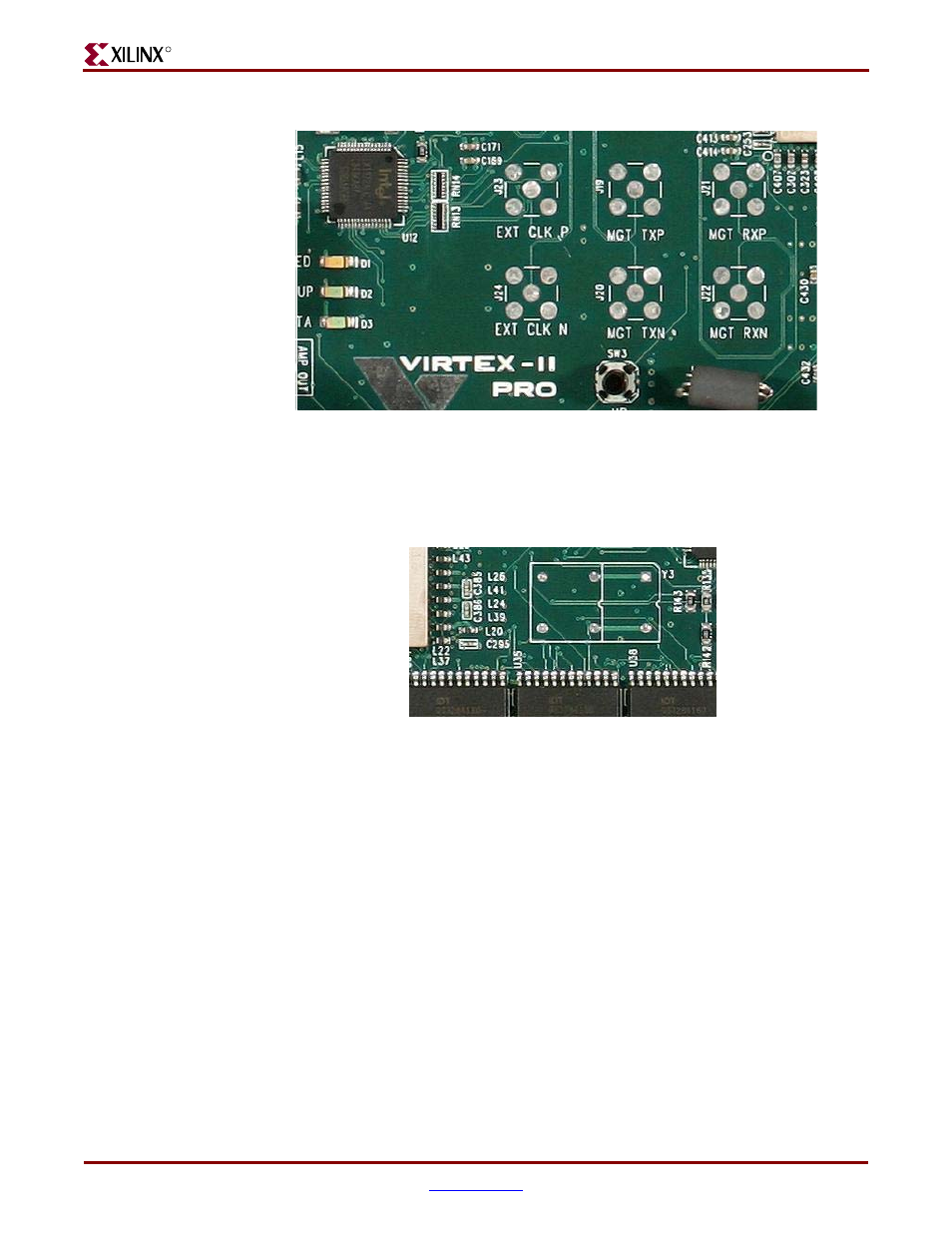
The alternate clock input is obtained from a user-supplied 3.3V oscillator. The footprint on
the printed circuit board supports either a full size (21mm x 13mm) or half size (13mm x
13mm) through-hole oscillator.
identifies the location of the alternate clock
input oscillator.
Using the DIMM Module DDR SDRAM
The XUP Virtex-II Pro Development System is equipped with a 184-pin Dual In-line
Memory Module (DIMM) socket that provides access up to 2 GB of Double Data Rate
SDRAM. The DDR SDRAM is an enhancement to the traditional Synchronous DRAM. It
supports data transfer on both edges of each clock cycle, effectively doubling the data
throughput of the memory device.
The DDR SDRAM operates with a differential clock: CLK and CLK_Z (the transition of
CLK going high and CLK_Z going low is considered the positive edge of the CLK)
commands (address and control signals) are registered at every positive edge of the CLK.
Input data is registered on both edges of the data strobe (DQS), and output data is
referenced to both edges of DQS, as well as both edges of CLK.
A bidirectional data strobe is transmitted by the DDR SDRAM during Reads and by the
FPGA DDR SDRAM memory controller during Writes. DQS is edge-aligned with the data
for Reads and center-aligned with the data for Writes.
Figure 2-4:
External Differential Clock Inputs
Figure 2-5:
Alternate Clock Input Oscillator