Figure 2-7, Figure 2-8, Figure 2-9 – Digilent 6003-410-000P-KIT User Manual
Page 26
26
XUP Virtex-II Pro Development System
UG069 (v1.0) March 8, 2005
Chapter 2: Using the System
R
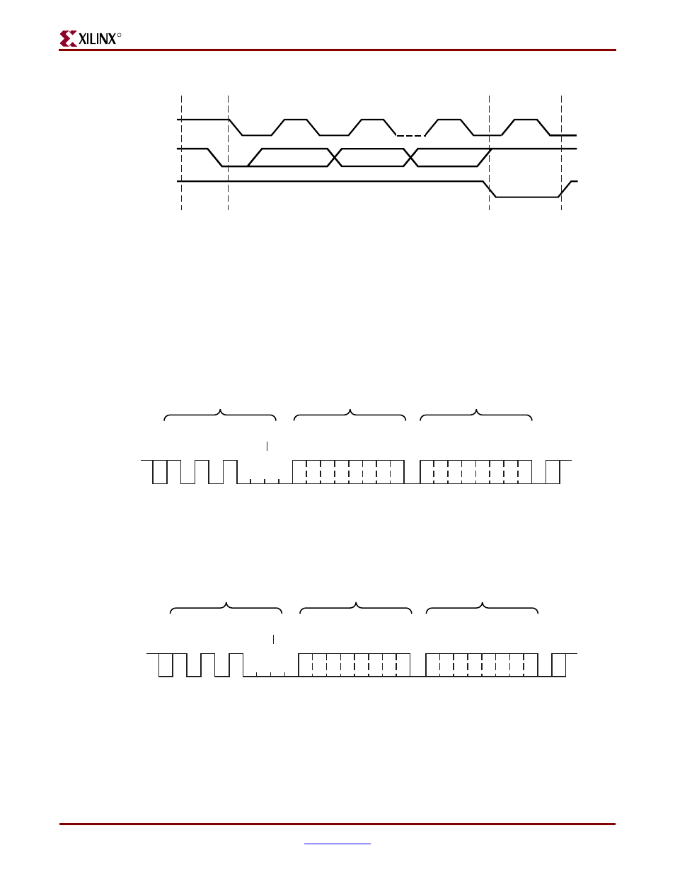
The SPD device always responds with an acknowledge after recognition of a start
condition and its slave address (100). If a read command was issued, the SPD device
transmits eight bits of data, releases the SDRAM_SDA data line, and monitors the
SDRAM_SDA data line for an acknowledge. If an acknowledge is detected and no stop bit is
generated by the master, the SPD device continues to transmit data. If no acknowledge is
detected, the SPD device terminates further data transmission and waits for the stop bit
condition to return to low power mode.
SPD device read and write operations are shown in
and
Figure 2-7:
Acknowledge Response from Receiver
SCL FROM
MASTER
SDA OUTPUT FROM
TRANSMITTER
SDA OUTPUT FROM
RECEIVER
START BIT
ACKNOWLEDGE
1
2
8
9
UG069_08_021405
Figure 2-8:
EEPROM Sequential Read
SLAVE ADDRESS
READ
DATA n
DATA n+1
MASTER
(FPGA)
SDRAM_SDA
SLAVE
(SPD EEPROM)
0
0
1
1
0
0
0
1
1
ACK
START
A2
A1
A0
R/W
ACK
ACK
STOP
UG069_09_021405
Figure 2-9:
EEPROM Write
SLAVE ADDRESS
WRITE
WORD ADDRESS
DATA
MASTER
(FPGA)
SDRAM_SDA
SLAVE
(SPD EEPROM)
0
0
1
1
0
0
0
1
1
ACK
START
A2
A1
A0
R/W
ACK
ACK
STOP
UG069_10_021405