Configuring the fpga, Figure 2-2, Chapter 2: using the system – Digilent 6003-410-000P-KIT User Manual
Page 20
20
XUP Virtex-II Pro Development System
UG069 (v1.0) March 8, 2005
Chapter 2: Using the System
R
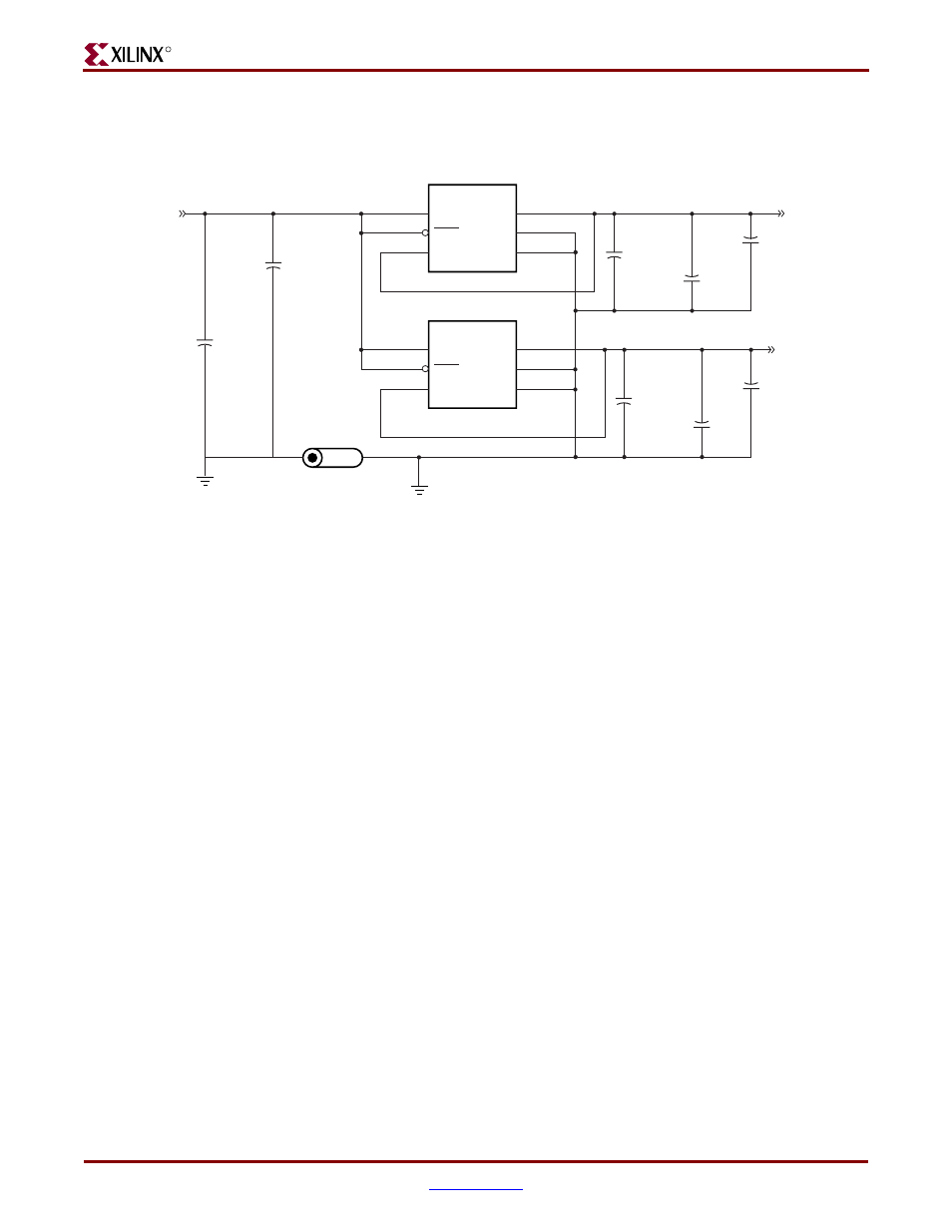
Because of the analog nature of the MGTs, the power for those elements are created by low
noise, low dropout linear regulators.
shows the power supply for the MGTs.
Configuring the FPGA
At power up, or when the RESET_RELOAD push button (SW1) is pressed for longer than
2 seconds, the FPGA begins to configure. The two configuration methods supported, JTAG
and master SelectMAP, are determined by the CONFIG SOURCE switch, the most
significant switch (left side) of SW9.
If the CONFIG SOURCE switch is closed, on, or up, a high-speed SelectMap byte-wide
configuration from the on-board Platform Flash configuration PROM (U3) is selected as
the configuration source. This is identified to the user through the illumination of the
PROM CONFIG LED (D19).
The Platform Flash configuration PROM supports two different FPGA configurations
(versions) selected by the position of the PROM VERSION switch, the least significant
switch (right side) of SW9.
If the PROM VERSION switch is closed, on, or up, the GOLDEN configuration from the on-
board Platform Flash configuration PROM is selected as the configuration data. This is
identified to the user through the illumination of the GOLDEN CONFIG LED (D14). This
configuration can be a board test utility provided by Xilinx, or another safe default
configuration. It is important to note that the PROM VERSION switch is only sampled on
board powerup and after a complete system reset. This means that if this switch is changed
after board powerup, the RESET_RELOAD pushbutton (SW1) must be pressed for more
than 2 seconds for the new state of the switch to be recognized.
If the PROM VERSION switch is open, off, or down, a User configuration from the on-board
Platform Flash configuration PROM is selected as the configuration data. This
configuration must be programmed into the Platform Flash PROM from the JTAG
Platform Cable USB interface or the USB interface following the instructions in
B, “Programming the Platform FLASH PROM User Area.”
Figure 2-2:
MGT Power
L32
FERRITE BEAD
2961666671
+
+
+
+
C431
C429
33OUF 6.3V
33OUF 6.3V
LT1963AEQ-25
GND_MGT
2
1
5
4
3
6
4
3
6
IN
OUT
SHDN
GND
TAB
SENSE
IN
OUT
SHDN
GND
TAB
SENSE
FIXED 2.5V LDO
FIXED 2.5V LDO
LT1963AEQ-25
U21
U20
2
5
1
C428
330UF 6.3V
C433
330UF 6.3V
C430
0.1UF
C434
C432
1000PF
C427
1000PF
0.1UF
VCC_MGT
VTT_MGT
VCC3V3
UG069_05_010605