Using the cpu debug port and cpu reset – Digilent 6003-410-000P-KIT User Manual
Page 58
58
XUP Virtex-II Pro Development System
UG069 (v1.0) March 8, 2005
Chapter 2: Using the System
R
Using the CPU Debug Port and CPU Reset
The CPU Debug port (J36) is a right angle header that provides connections to the
debugging resources of the PowerPC 405 CPU core.
The PowerPC 405 CPU cores include dedicated debug resources that support a variety of
debug modes for debugging during hardware and software development. These debug
resources include:
•
Internal debug mode for use by ROM monitors and software debuggers
•
External debug mode for use by JTAG debuggers
•
Debug wait mode, which allows the servicing of interrupts while the processor
appears to be stopped
•
Real-time trace mode, which supports event triggering for real time tracing
Debug modes and events are controlled using debug registers in the processor. The debug
registers are accessed either through software running on the processor or through the
JTAG port. The debug modes, events, controls, and interfaces provide a powerful
combination of debug resources for hardware and software development tools.
The JTAG port interface supports the attachment of external debug tools, such as the
powerful ChipScope™ Integrated Logic Analyzer, a powerful tool providing logic
analyzer capabilities for signals inside an FPGA, without the need for expensive external
instrumentation. Using the JTAG test access port, a debug tool can single-step the
processor and examine the internal processor state to facilitate software debugging. This
capability complies with standard JTAG hardware for boundary scan system testing.
External debug mode can be used to alter normal program execution. It provides the
ability to debug system hardware as well as software. The mode supports multiple
functions: starting and stopping the processor, single-stepping instruction execution,
setting breakpoints, as well as monitoring processor status. Access to processor resources
is provided through the CPU Debug Port.
The PPC405 JTAG Debug Port supports the four required JTAG signals: CPU_TCK,
CPU_TMS, CPU_TDO, and CPU_TDI. It also implements the optional CPU_TRST signal.
The frequency of the JTAG clock signal, CPU_TCK, can range from 0 MHz up to one-half
of the processor clock frequency. The JTAG debug port logic is reset at the same time the
system is reset, using the CPU_TRST signal. When CPU_TRST is asserted, the JTAG TAP
controller returns to the test-logic reset state.
B04
FPGA_TCK
–
–
–
B05-B45
GND
–
–
–
B46
HS_CLKIN
B16 (GCLK6S)
No_Pair
LVCMOS25
B47
GND
–
–
–
B48
HS_CLKIO
E3
33P_2
LVTTL
B49
VCC5V5
–
–
–
B50
SHIELD
–
–
–
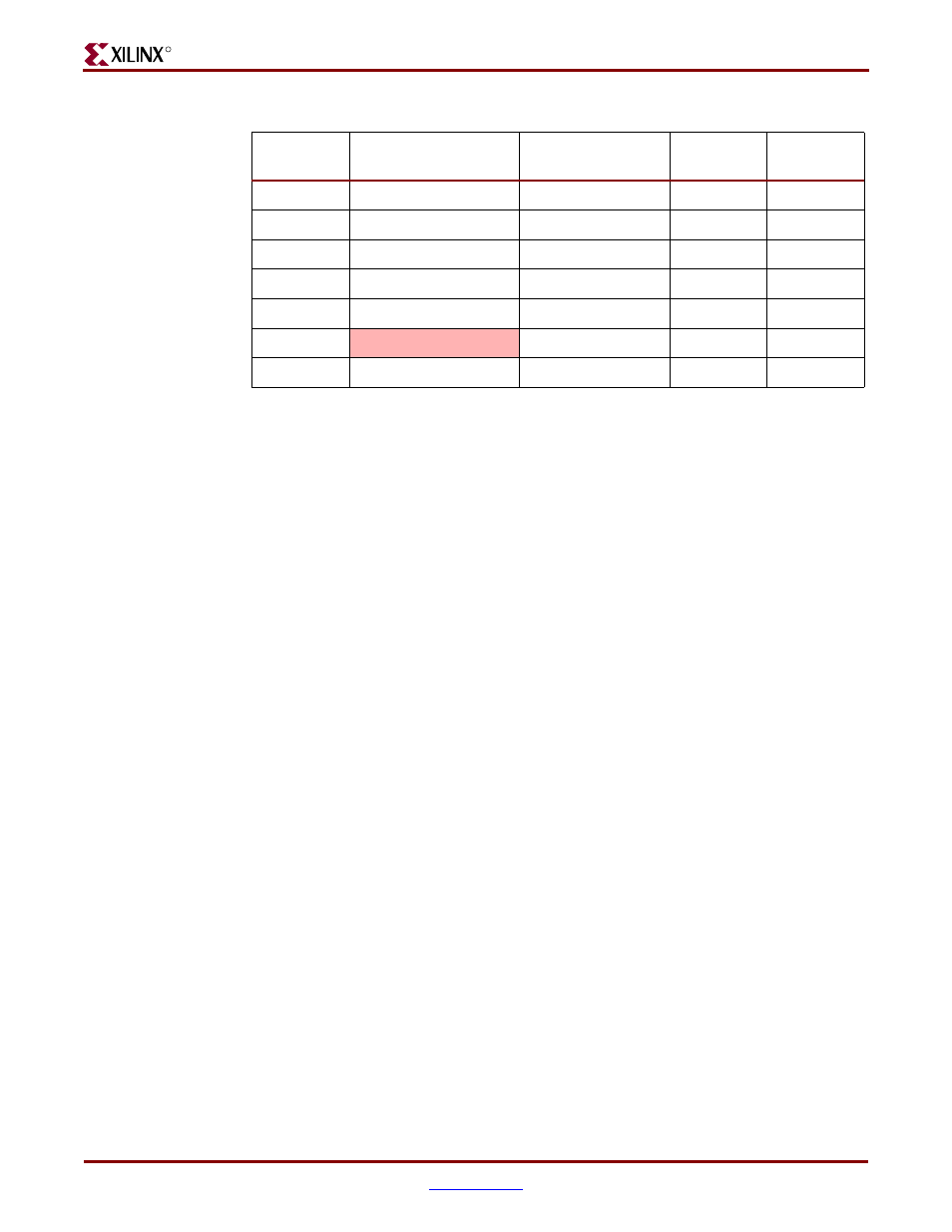
Table 2-16:
High-Speed Digilent Expansion Connector Pinout (Continued)
J37
PIN
Signal
FPGA
Pin
Differential
Pair
I/O Type