Timer/counter timing diagrams, Atmega169v/l – Rainbow Electronics Atmega169L User Manual
Page 87
87
ATmega169V/L
2514A–AVR–08/02
Timer/Counter Timing
Diagrams
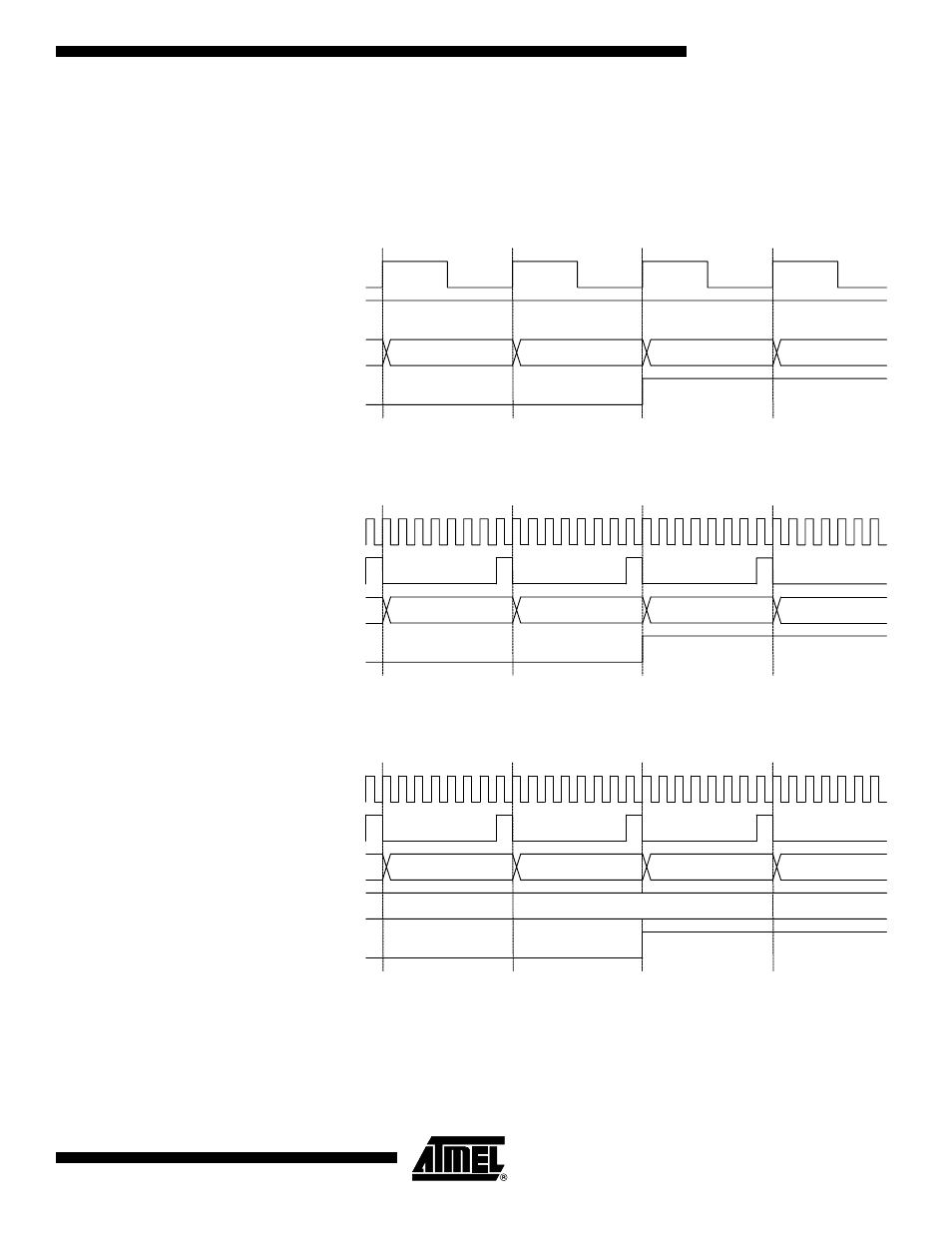
The Timer/Counter is a synchronous design and the timer clock (clk
T0
) is therefore
shown as a clock enable signal in the following figures. The figures include information
on when interrupt flags are set. Figure 33 contains timing data for basic Timer/Counter
operation. The figure shows the count sequence close to the MAX value in all modes
other than phase correct PWM mode.
Figure 33. Timer/Counter Timing Diagram, no Prescaling
Figure 34 shows the same timing data, but with the prescaler enabled.
Figure 34. Timer/Counter Timing Diagram, with Prescaler (f
clk_I/O
/8)
Figure 35 shows the setting of OCF0A in all modes except CTC mode.
Figure 35. Timer/Counter Timing Diagram, Setting of OCF0A, with Prescaler (f
clk_I/O
/8)
clk
Tn
(clk
I/O
/1)
TOVn
clk
I/O
TCNTn
MAX - 1
MAX
BOTTOM
BOTTOM + 1
TOVn
TCNTn
MAX - 1
MAX
BOTTOM
BOTTOM + 1
clk
I/O
clk
Tn
(clk
I/O
/8)
OCFnx
OCRnx
TCNTn
OCRnx Value
OCRnx - 1
OCRnx
OCRnx + 1
OCRnx + 2
clk
I/O
clk
Tn
(clk
I/O
/8)