Adc multiplexer selection register – admux, Atmega169v/l – Rainbow Electronics Atmega169L User Manual
Page 204
204
ATmega169V/L
2514A–AVR–08/02
Example: ADMUX = 0xFB (ADC3 - ADC2, 1.1V reference, left adjusted result)
Voltage on ADC3 is 300 mV, voltage on ADC2 is 500 mV.
ADCR = 512 * (300 - 500) / 1100 = -93 = 0x3A3.
ADCL will thus read 0xC0, and ADCH will read 0xD8. Writing zero to ADLAR right
adjusts the result: ADCL = 0xA3, ADCH = 0x03.
ADC Multiplexer Selection
Register – ADMUX
• Bit 7:6 – REFS1:0: Reference Selection Bits
These bits select the voltage reference for the ADC, as shown in Table 89. If these bits
are changed during a conversion, the change will not go in effect until this conversion is
complete (ADIF in ADCSRA is set). The internal voltage reference options may not be
used if an external reference voltage is being applied to the AREF pin.
•
Bit 5 – ADLAR: ADC Left Adjust Result
The ADLAR bit affects the presentation of the ADC conversion result in the ADC Data
Register. Write one to ADLAR to left adjust the result. Otherwise, the result is right
adjusted. Changing the ADLAR bit will affect the ADC Data Register immediately,
regardless of any ongoing conversions. For a complete description of this bit, see “The
ADC Data Register – ADCL and ADCH” on page 207.
Table 88. Correlation Between Input Voltage and Output Codes
V
ADCn
Read Code
Corresponding Decimal Value
V
ADCm
+ V
REF
0x1FF
511
V
ADCm
+ 0.999 V
REF
0x1FF
511
V
ADCm
+ 0.998 V
REF
0x1FE
510
...
...
...
V
ADCm
+ 0.001 V
REF
0x001
1
V
ADCm
0x000
0
V
ADCm
- 0.001 V
REF
0x3FF
-1
...
...
...
V
ADCm
- 0.999 V
REF
0x201
-511
V
ADCm
- V
REF
0x200
-512
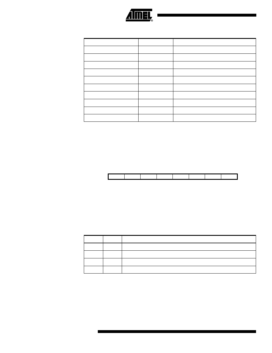
Bit
7
6
5
4
3
2
1
0
REFS1
REFS0
ADLAR
MUX4
MUX3
MUX2
MUX1
MUX0
ADMUX
Read/Write
R/W
R/W
R/W
R/W
R/W
R/W
R/W
R/W
Initial Value
0
0
0
0
0
0
0
0
Table 89. Voltage Reference Selections for ADC
REFS1
REFS0
Voltage Reference Selection
0
0
AREF, Internal Vref turned off
0
1
AVCC with external capacitor at AREF pin
1
0
Reserved
1
1
Internal 1.1V Voltage Reference with external capacitor at AREF pin