Synchronous clock operation, Frame formats, Atmega169v/l – Rainbow Electronics Atmega169L User Manual
Page 154
154
ATmega169V/L
2514A–AVR–08/02
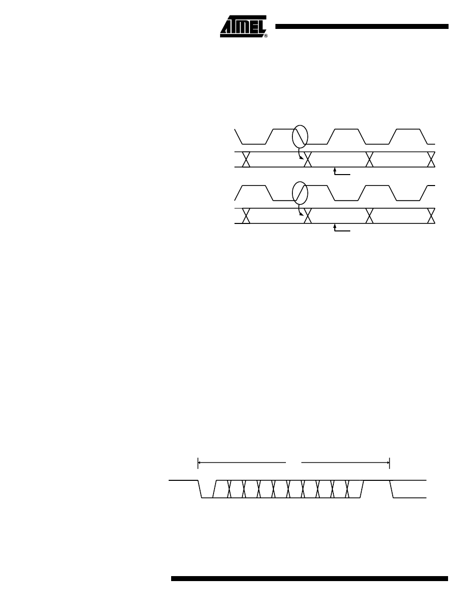
Synchronous Clock Operation
When synchronous mode is used (UMSEL = 1), the XCK pin will be used as either clock
input (Slave) or clock output (Master). The dependency between the clock edges and
data sampling or data change is the same. The basic principle is that data input (on
RxD) is sampled at the opposite XCK clock edge of the edge the data output (TxD) is
changed.
Figure 70. Synchronous Mode XCK Timing.
The UCPOL bit UCRSC selects which XCK clock edge is used for data sampling and
which is used for data change. As Figure 70 shows, when UCPOL is zero the data will
be changed at rising XCK edge and sampled at falling XCK edge. If UCPOL is set, the
data will be changed at falling XCK edge and sampled at rising XCK edge.
Frame Formats
A serial frame is defined to be one character of data bits with synchronization bits (start
and stop bits), and optionally a parity bit for error checking. The USART accepts all 30
combinations of the following as valid frame formats:
•
1 start bit
•
5, 6, 7, 8, or 9 data bits
•
no, even or odd parity bit
•
1 or 2 stop bits
A frame starts with the start bit followed by the least significant data bit. Then the next
data bits, up to a total of nine, are succeeding, ending with the most significant bit. If
enabled, the parity bit is inserted after the data bits, before the stop bits. When a com-
plete frame is transmitted, it can be directly followed by a new frame, or the
communication line can be set to an idle (high) state. Figure 71 illustrates the possible
combinations of the frame formats. Bits inside brackets are optional.
Figure 71. Frame Formats
St
Start bit, always low.
(n)
Data bits (0 to 8).
P
Parity bit. Can be odd or even.
RxD / TxD
XCK
RxD / TxD
XCK
UCPOL = 0
UCPOL = 1
Sample
Sample
1
0
2
3
4
[5]
[6]
[7]
[8]
[P]
St
Sp1 [Sp2]
(St / IDLE)
(IDLE)
FRAME