Atmega169 boundary- scan order, Atmega169v/l – Rainbow Electronics Atmega169L User Manual
Page 245
245
ATmega169V/L
2514A–AVR–08/02
ATmega169 Boundary-
scan Order
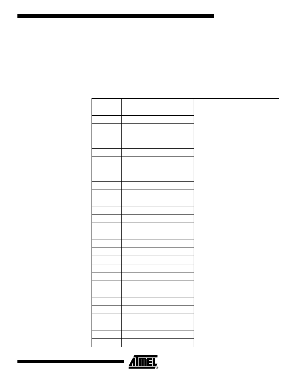
Table 107 shows the Scan order between TDI and TDO when the Boundary-scan chain
is selected as data path. Bit 0 is the LSB; the first bit scanned in, and the first bit
scanned out. The scan order follows the pin-out order as far as possible. Therefore, the
bits of Port A is scanned in the opposite bit order of the other ports. Exceptions from the
rules are the Scan chains for the analog circuits, which constitute the most significant
bits of the scan chain regardless of which physical pin they are connected to. In Figure
108, PXn. Data corresponds to FF0, PXn. Control corresponds to FF1, and PXn.
Pullup_enable corresponds to FF2. Bit 2, 3, 4, and 5 of Port C is not in the scan chain,
since these pins constitute the TAP pins when the JTAG is enabled.
Table 107. ATmega169 Boundary-scan Order
Bit Number
Signal Name
Module
197
AC_IDLE
Comparator
196
ACO
195
ACME
194
AINBG
193
COMP
ADC
192
ACLK
191
ACTEN
190
ADHSM
189
ADCBGEN
188
ADCEN
187
AMPEN
186
DAC_9
185
DAC_8
184
DAC_7
183
DAC_6
182
DAC_5
181
DAC_4
180
DAC_3
179
DAC_2
178
DAC_1
177
DAC_0
176
EXTCH
175
GNDEN
174
HOLD
173
IREFEN
172
MUXEN_7
171
MUXEN_6
170
MUXEN_5
169
MUXEN_4