Adc control and status register b – adcsrb, Digital input disable register 1 – didr1, Atmega169v/l – Rainbow Electronics Atmega169L User Manual
Page 208
208
ATmega169V/L
2514A–AVR–08/02
• ADC9:0: ADC Conversion Result
These bits represent the result from the conversion, as detailed in “ADC Conversion
Result” on page 203.
ADC Control and Status
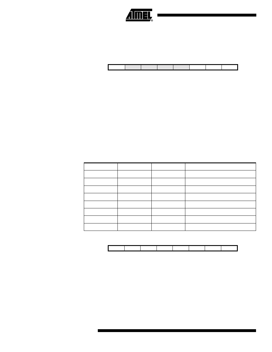
Register B – ADCSRB
• Bit 7 – ADHSM: ADC High Speed Mode
Writing this bit to one enables the ADC High Speed mode. This mode enables higher
conversion rate at the expense of higher power consumption.
• Bit 2:0 – ADTS2:0: ADC Auto Trigger Source
If ADATE in ADCSRA is written to one, the value of these bits selects which source will
trigger an ADC conversion. If ADATE is cleared, the ADTS2:0 settings will have no
effect. A conversion will be triggered by the rising edge of the selected interrupt flag.
Note that switching from a trigger source that is cleared to a trigger source that is set,
will generate a positive edge on the trigger signal. If ADEN in ADCSRA is set, this will
start a conversion. Switching to Free Running mode (ADTS[2:0]=0) will not cause a trig-
ger event, even if the ADC Interrupt Flag is set
.
Digital Input Disable Register
1 – DIDR1
• Bit 7..0 – ADC7D..ADC0D: ADC7..0 Digital Input Disable
When this bit is written logic one, the digital input buffer on the corresponding ADC pin is
disabled. The corresponding PIN Register bit will always read as zero when this bit is
set. When an analog signal is applied to the ADC7..0 pin and the digital input from this
pin is not needed, this bit should be written logic one to reduce power consumption in
the digital input buffer.
Bit
7
6
5
4
3
2
1
0
ADHSM
ACME
–
–
–
ADTS2
ADTS1
ADTS0
ADCSRB
Read/Write
R/W
R/W
R
R
R
R/W
R/W
R/W
Initial Value
0
0
0
0
0
0
0
0
Table 92. ADC Auto Trigger Source Selections
ADTS2
ADTS1
ADTS0
Trigger Source
0
0
0
Free Running mode
0
0
1
Analog Comparator
0
1
0
External Interrupt Request 0
0
1
1
Timer/Counter0 Compare Match
1
0
0
Timer/Counter0 Overflow
1
0
1
Timer/Counter Compare Match B
1
1
0
Timer/Counter1 Overflow
1
1
1
Timer/Counter1 Capture Event
Bit
7
6
5
4
3
2
1
0
ADC7D
ADC6D
ADC5D
ADC4D
ADC3D
ADC2D
ADC1D
ADC0D
DIDR1
Read/Write
R/W
R/W
R/W
R/W
R/W
R/W
R/W
R/W
Initial Value
0
0
0
0
0
0
0
0