Output compare unit, Atmega169v/l, Data bus – Rainbow Electronics Atmega169L User Manual
Page 80
80
ATmega169V/L
2514A–AVR–08/02
Depending of the mode of operation used, the counter is cleared, incremented, or dec-
remented at each timer clock (clk
T0
). clk
T0
can be generated from an external or internal
clock source, selected by the Clock Select bits (CS02:0). When no clock source is
selected (CS02:0 = 0) the timer is stopped. However, the TCNT0 value can be accessed
by the CPU, regardless of whether clk
T0
is present or not. A CPU write overrides (has
priority over) all counter clear or count operations.
The counting sequence is determined by the setting of the WGM01 and WGM00 bits
located in the Timer/Counter Control Register (TCCR0A). There are close connections
between how the counter behaves (counts) and how waveforms are generated on the
Output Compare output OC0A. For more details about advanced counting sequences
and waveform generation, see “Modes of Operation” on page 83.
The Timer/Counter Overflow Flag (TOV0) is set according to the mode of operation
selected by the WGM01:0 bits. TOV0 can be used for generating a CPU interrupt.
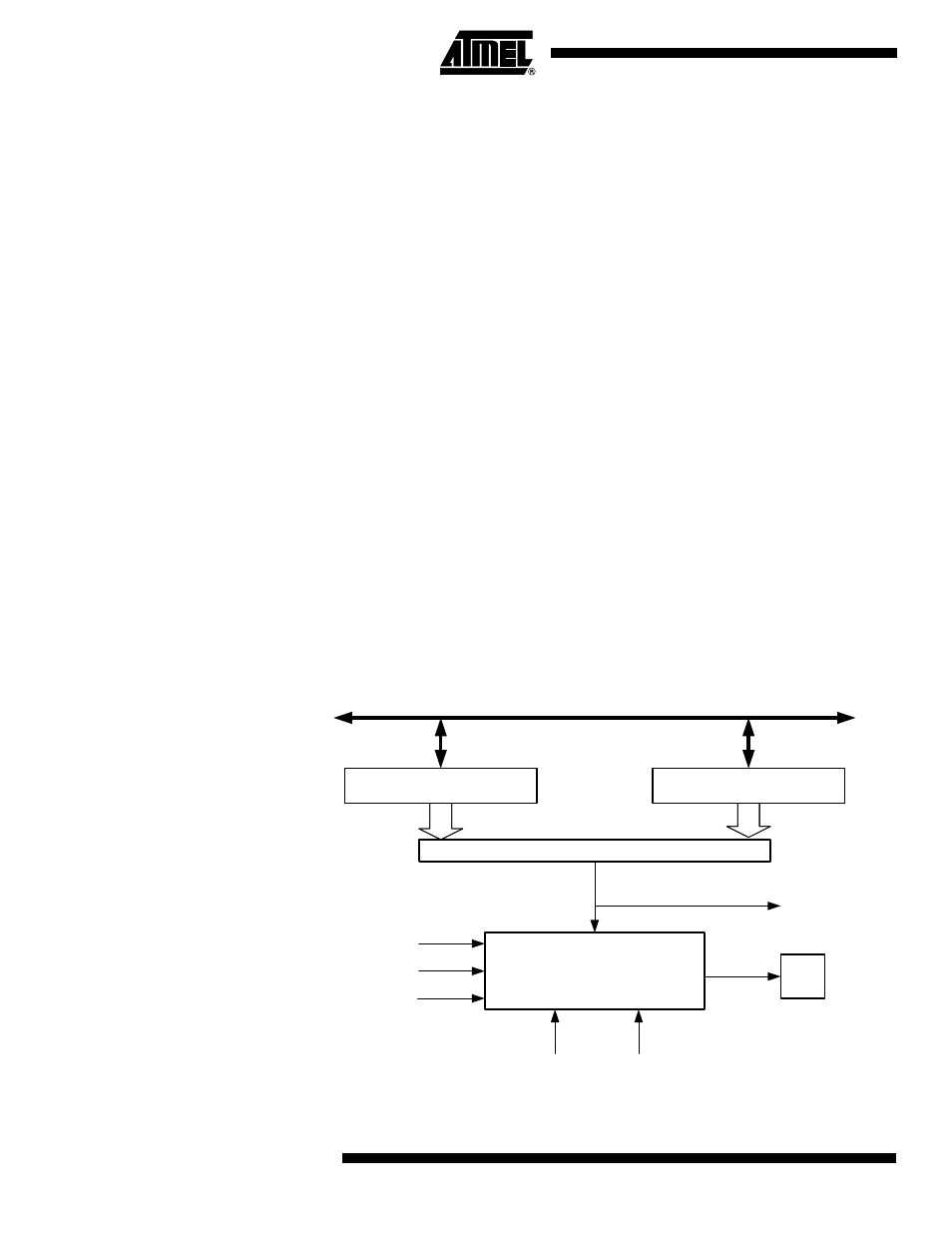
Output Compare Unit
The 8-bit comparator continuously compares TCNT0 with the Output Compare Register
(OCR0A). Whenever TCNT0 equals OCR0A, the comparator signals a match. A match
will set the Output Compare Flag (OCF0A) at the next timer clock cycle. If enabled
(OCIE0A = 1 and Global Interrupt Flag in SREG is set), the Output Compare Flag gen-
erates an Output Compare interrupt. The OCF0A flag is automatically cleared when the
interrupt is executed. Alternatively, the OCF0A flag can be cleared by software by writ-
ing a logical one to its I/O bit location. The Waveform Generator uses the match signal
to generate an output according to operating mode set by the WGM01:0 bits and Com-
pare Output mode (COM0A1:0) bits. The max and bottom signals are used by the
Waveform Generator for handling the special cases of the extreme values in some
modes of operation (See “Modes of Operation” on page 83.).
Figure 28 shows a block diagram of the Output Compare unit.
Figure 28. Output Compare Unit, Block Diagram
OCFnx (Int.Req.)
=
(8-bit Comparator )
OCRnx
OCnx
DATA BUS
TCNTn
WGMn1:0
Waveform Generator
top
FOCn
COMnX1:0
bottom