External clock drive waveforms, External clock drive, Spi timing characteristics – Rainbow Electronics Atmega169L User Manual
Page 298: Atmega169v/l, External clock drive spi timing characteristics
298
ATmega169V/L
2514A–AVR–08/02
External Clock Drive
Waveforms
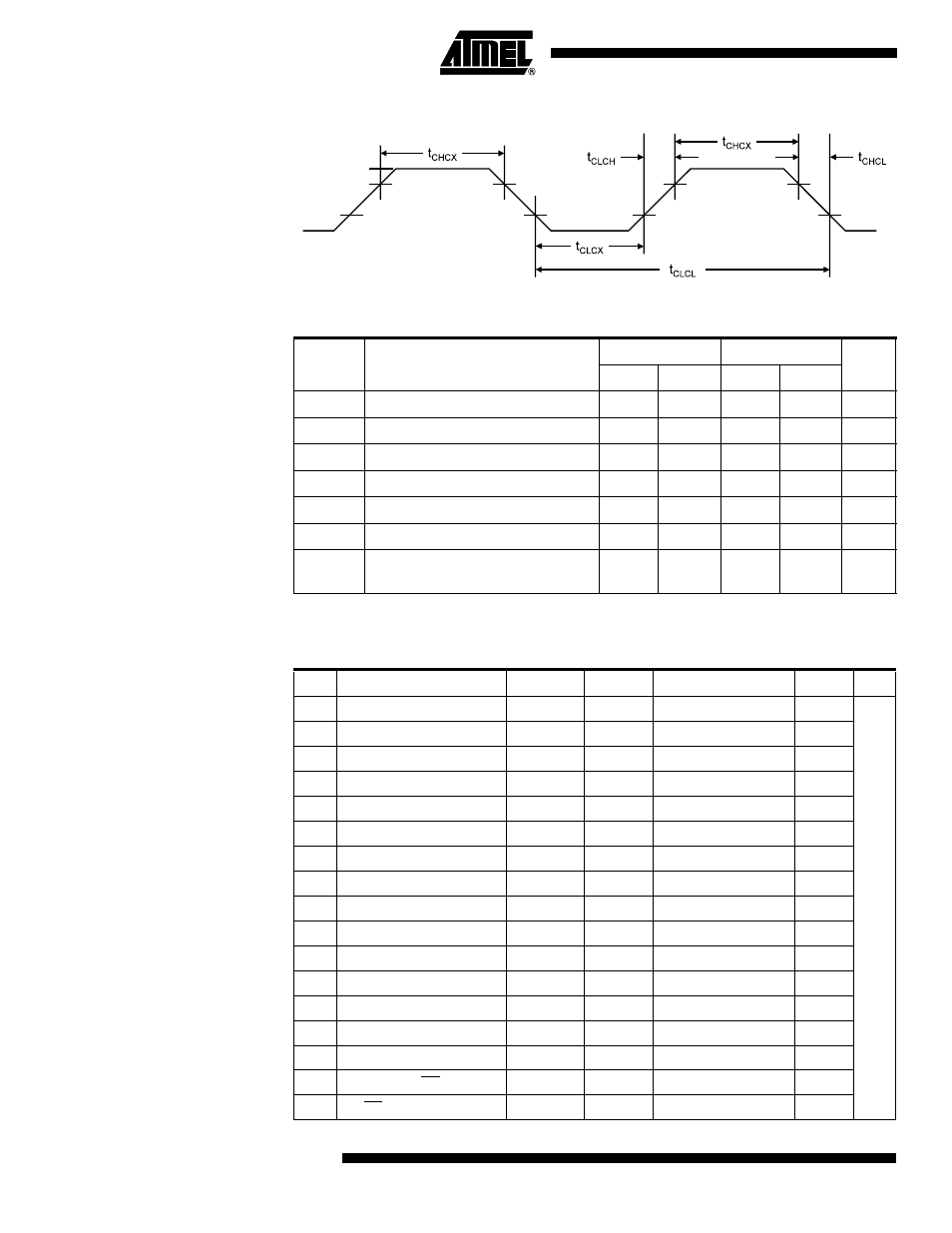
Figure 135. External Clock Drive Waveforms
External Clock Drive
SPI Timing
Characteristics
See Figure 136 and Figure 137 for details.
V
IL1
V
IH1
Table 133. External Clock Drive
Symbol
Parameter
V
CC
= 1.8 - 3.6V
V
CC
= 2.7 - 3.6V
Units
Min.
Max.
Min.
Max.
1/t
CLCL
Oscillator Frequency
0
TBD
0
TBD
MHz
t
CLCL
Clock Period
TBD
TBD
ns
t
CHCX
High Time
TBD
TBD
ns
t
CLCX
Low Time
TBD
TBD
ns
t
CLCH
Rise Time
TBD
TBD
µs
t
CHCL
Fall Time
TBD
TBD
µs
∆
t
CLCL
Change in period from one clock
cycle to the next
2
2
%
Table 134. SPI Timing Parameters
Description
Mode
Min
Typ
Max
1
SCK period
Master
See Table 69
ns
2
SCK high/low
Master
50% duty cycle
3
Rise/Fall time
Master
TBD
4
Setup
Master
TBD
5
Hold
Master
TBD
6
Out to SCK
Master
TBD
7
SCK to out
Master
TBD
8
SCK to out high
Master
TBD
9
SS low to out
Slave
TBD
10
SCK period
Slave
4 • t
ck
TBD
11
SCK high/low
Slave
2 • t
ck
TBD
12
Rise/Fall time
Slave
TBD
13
Setup
Slave
TBD
14
Hold
Slave
TBD
15
SCK to out
Slave
TBD
16
SCK to SS high
Slave
TBD
17
SS high to tri-state
Slave
TBD