Analog noise canceling techniques, Offset compensation schemes, Atmega169v/l – Rainbow Electronics Atmega169L User Manual
Page 200
200
ATmega169V/L
2514A–AVR–08/02
Analog Noise Canceling
Techniques
Digital circuitry inside and outside the device generates EMI which might affect the
accuracy of analog measurements. If conversion accuracy is critical, the noise level can
be reduced by applying the following techniques:
1.
Keep analog signal paths as short as possible. Make sure analog tracks run
over the analog ground plane, and keep them well away from high-speed
switching digital tracks.
2.
The AVCC pin on the device should be connected to the digital V
CC
supply
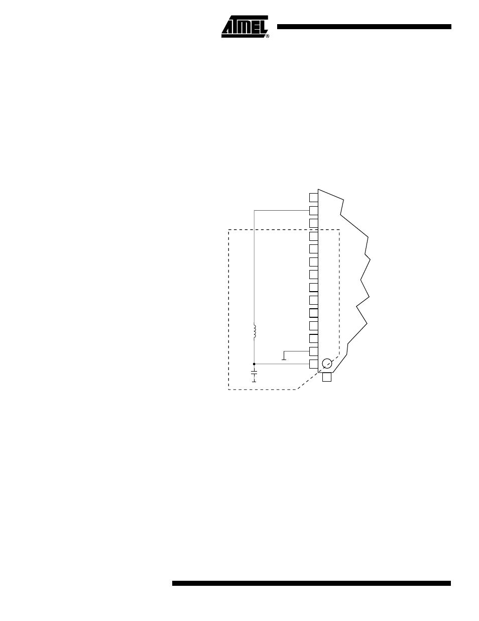
voltage via an LC network as shown in Figure 90.
3.
Use the ADC noise canceler function to reduce induced noise from the CPU.
4.
If any ADC port pins are used as digital outputs, it is essential that these do
not switch while a conversion is in progress.
Figure 90. ADC Power Connections
Offset Compensation
Schemes
Thestage has a built-in offset cancellation circuitry that nulls the offset of differential
measurements as much as possible. The remaining offset in the analog path can be
measured directly by selecting the same channel for both differential inputs. This offset
residue can be then subtracted in software from the measurement results. Using this
kind of software based offset correction, offset on any channel can be reduced below
one LSB.
VCC
GND
100nF
Analog Ground Plane
(ADC0) PF0
(ADC7) PF7
(ADC1) PF1
(ADC2) PF2
(ADC3) PF3
(ADC4) PF4
(ADC5) PF5
(ADC6) PF6
AREF
GND
AVCC
52
53
54
55
56
57
58
59
60
61
61
62
62
63
63
64
64
1
51
LCDCAP
PA0
10
µΗ