Analog input circuitry, Atmega169v/l – Rainbow Electronics Atmega169L User Manual
Page 199
199
ATmega169V/L
2514A–AVR–08/02
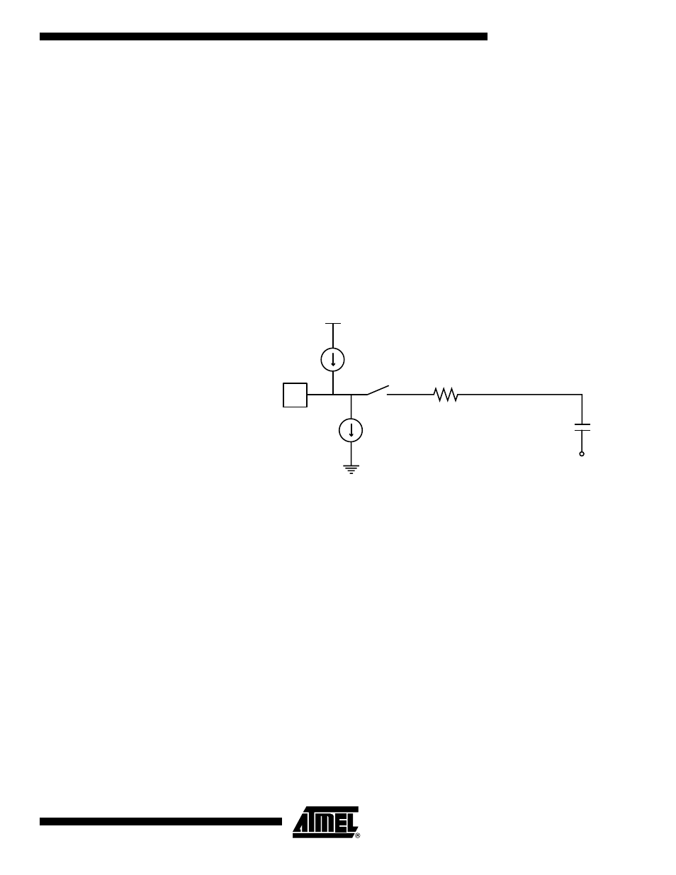
Analog Input Circuitry
The analog input circuitry for single ended channels is illustrated in Figure 89. An analog
source applied to ADCn is subjected to the pin capacitance and input leakage of that
pin, regardless of whether that channel is selected as input for the ADC. When the chan-
nel is selected, the source must drive the S/H capacitor through the series resistance
(combined resistance in the input path).
The ADC is optimized for analog signals with an output impedance of approximately
10 k
Ω or less. If such a source is used, the sampling time will be negligible. If a source
with higher impedance is used, the sampling time will depend on how long time the
source needs to charge the S/H capacitor, with can vary widely. The user is recom-
mended to only use low impedant sources with slowly varying signals, since this
minimizes the required charge transfer to the S/H capacitor.
Signal components higher than the Nyquist frequency (f
ADC
/2) should not be present for
either kind of channels, to avoid distortion from unpredictable signal convolution. The
user is advised to remove high frequency components with a low-pass filter before
applying the signals as inputs to the ADC.
Figure 89. Analog Input Circuitry
ADCn
I
IH
1..100 k
Ω
C
S/H
= 14 pF
V
CC
/2
I
IL