Latching of fuses, Signature bytes, Calibration byte – Rainbow Electronics Atmega169L User Manual
Page 268: Signal names, Atmega169v/l
268
ATmega169V/L
2514A–AVR–08/02
Latching of Fuses
The fuse values are latched when the device enters programming mode and changes of
the fuse values will have no effect until the part leaves Programming mode. This does
not apply to the EESAVE Fuse which will take effect once it is programmed. The fuses
are also latched on Power-up in Normal mode.
Signature Bytes
All Atmel microcontrollers have a three-byte signature code which identifies the device.
This code can be read in both serial and parallel mode, also when the device is locked.
The three bytes reside in a separate address space.
For the ATmega169 the signature bytes are:
1.
0x000: 0x1E (indicates manufactured by Atmel).
2.
0x001: 0x94 (indicates 16KB Flash memory).
3.
0x002: 0x05 (indicates ATmega169 device when 0x001 is 0x94).
Calibration Byte
The ATmega169 has a byte calibration value for the internal RC Oscillator. This byte
resides in the high byte of address 0x000 in the signature address space. During reset,
this byte is automatically written into the OSCCAL Register to ensure correct frequency
of the calibrated RC Oscillator.
Parallel Programming
Parameters, Pin
Mapping, and
Commands
This section describes how to parallel program and verify Flash Program memory,
EEPROM Data memory, Memory Lock bits, and Fuse bits in the ATmega169. Pulses
are assumed to be at least 250 ns unless otherwise noted.
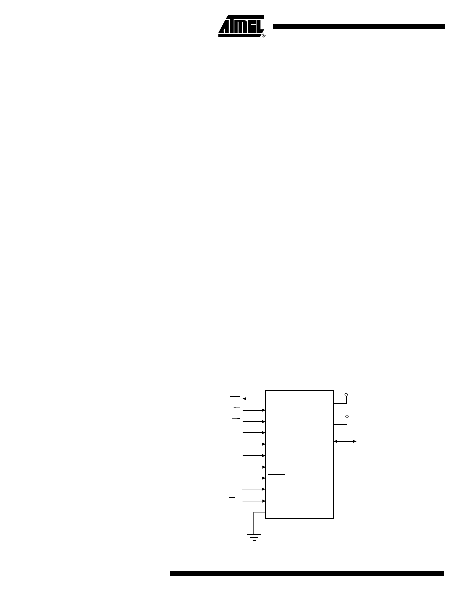
Signal Names
In this section, some pins of the ATmega169 are referenced by signal names describing
their functionality during parallel programming, see Figure 118 and Table 121. Pins not
described in the following table are referenced by pin names.
The XA1/XA0 pins determine the action executed when the XTAL1 pin is given a posi-
tive pulse. The bit coding is shown in Table 123.
When pulsing WR or OE, the command loaded determines the action executed. The dif-
ferent Commands are shown in Table 124.
Figure 118. Parallel Programming
VCC
+5V
GND
XTAL1
PD1
PD2
PD3
PD4
PD5
PD6
PB7 - PB0
DATA
RESET
PD7
+12 V
BS1
XA0
XA1
OE
RDY/BSY
PAGEL
PA0
WR
BS2
AVCC
+5V