Lcd control and status register b – lcdcrb, Atmega169v/l – Rainbow Electronics Atmega169L User Manual
Page 220
220
ATmega169V/L
2514A–AVR–08/02
LCD Control and Status
Register B – LCDCRB
• Bit 7 – LCDCS: LCD Clock Select
When this bit is written to zero, the system clock is used. When this bit is written to one,
the external asynchronous clock source is used. The asynchronous clock source is
either Timer/Counter Oscillator or external clock, depending on EXCLK in ASSR. See
“Asynchronous operation of the Timer/Counter” on page 137 for futher details.
• Bit 6 – LCD2B: LCD 1/2 Bias Select
When this bit is written to zero, 1/3 bias is used. When this bit is written to one, ½ bias is
used. Refer to the LCD Manufacture for recommended bias selection.
• Bit 5:4 – LCDMUX1:0: LCD Mux Select
The LCDMUX1:0 bits determine the duty cycle. Common pins that are not used are ordi-
nary port pins. The different duty selections are shown in Table 94.
Note:
1. 1/2 bias when LCD2B is written to one and 1/3 otherwise.
• Bit 3 – Res: Reserved Bit
This bit is reserved bit in the ATmega169 and will always read as zero.
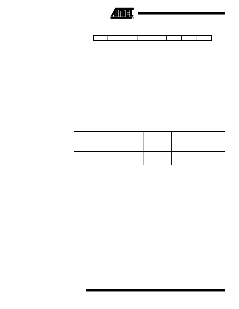
Bit
7
6
5
4
3
2
1
0
LCDCS
LCD2B
LCDMUX1
LCDMUX0
–
LCDPM2
LCDPM1
LCDPM0
LCDCRB
Read/Write
R/W
R/W
R/W
R/W
R
R/W
R/W
R/W
Initial Value
0
0
0
0
0
0
0
0
Table 94. LCD Duty Select
LCDMUX1
LCDMUX0
Duty
Bias
COM Pin
I/O Port Pin
0
0
Static
Static
COM0
COM1:3
0
1
1/2
1/2 or 1/3
(1)
COM0:1
COM2:3
1
0
1/3
1/2 or 1/3
(1)
COM0:2
COM3
1
1
1/4
1/2 or 1/3
(1)
COM0:3
None