Atmega169v/l, Dc characteristics – Rainbow Electronics Atmega169L User Manual
Page 297
297
ATmega169V/L
2514A–AVR–08/02
Note:
1. “Max” means the highest value where the pin is guaranteed to be read as low
2. “Min” means the lowest value where the pin is guaranteed to be read as high
3. Although each I/O port can sink more than the test conditions (10 mA at V
CC
= 3V) under steady state conditions (non-tran-
sient), the following must be observed:
TQFP Package:
1] The sum of all IOL, for all ports, should not exceed 400 mA.
2] The sum of all IOL, for ports A0 - A7, should not exceed 100 mA.
3] The sum of all IOL, for ports B0 - B3, should not exceed 100 mA.
4] The sum of all IOL, for ports B4 - B7, should not exceed 100 mA.
5] The sum of all IOL, for ports C0 - C3, should not exceed 100 mA.
6] The sum of all IOL, for ports C4 - C7, should not exceed 100 mA.
7] The sum of all IOL, for ports D0 - D3 and XTAL2, should not exceed 100 mA.
8] The sum of all IOL, for ports D4 - D7, should not exceed 100 mA
If IOL exceeds the test condition, VOL may exceed the related specification. Pins are not guaranteed to sink current greater
than the listed test condition.
4. Although each I/O port can source more than the test conditions (10 mA at V
CC
= 3V) under steady state conditions (non-
transient), the following must be observed:
TQFP Package:
1] The sum of all IOH, for all ports, should not exceed 400 mA.
2] The sum of all IOH, for ports A0 - A7, should not exceed 100 mA.
3] The sum of all IOH, for ports B0 - B3, should not exceed 100 mA.
4] The sum of all IOH, for ports B4 - B7, should not exceed 100 mA.
5] The sum of all IOH, for ports C0 - C3, should not exceed 100 mA.
6] The sum of all IOH, for ports C4 - C7, should not exceed 100 mA.
7] The sum of all IOH, for ports D0 - D3 and XTAL2, should not exceed 100 mA.
8] The sum of all IOH, for ports D4 - D7, should not exceed 100 mA
If IOH exceeds the test condition, VOH may exceed the related specification. Pins are not guaranteed to source current
greater than the listed test condition.
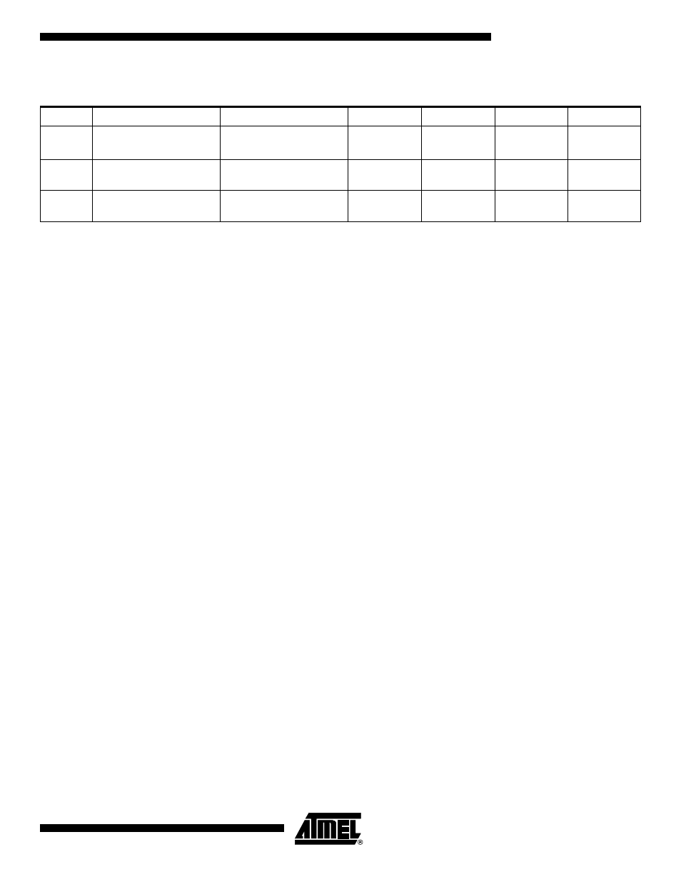
V
ACIO
Analog Comparator
Input Offset Voltage
V
CC
= 3V
V
in
= V
CC
/2
TBD
mV
I
ACLK
Analog Comparator
Input Leakage Current
V
CC
= 3V
V
in
= V
CC
/2
TBD
TBD
nA
t
ACID
Analog Comparator
Propagation Delay
V
CC
= 1.8V
V
CC
= 2.7V
TBD
TBD
ns
DC Characteristics
T
A
= -40
°C to 85°C, V
CC
= 1.8V to 3.6V (unless otherwise noted) (Continued)
Symbol
Parameter
Condition
Min.
Typ.
Max.
Units