The adc data register – adcl and adch, Adlar = 0, Adlar = 1 – Rainbow Electronics Atmega169L User Manual
Page 207: Atmega169v/l
207
ATmega169V/L
2514A–AVR–08/02
• Bits 2:0 – ADPS2:0: ADC Prescaler Select Bits
These bits determine the division factor between the XTAL frequency and the input
clock to the ADC.
The ADC Data Register –
ADCL and ADCH
ADLAR = 0
ADLAR = 1
When an ADC conversion is complete, the result is found in these two registers. If differ-
ential channels are used, the result is presented in two’s complement form.
When ADCL is read, the ADC Data Register is not updated until ADCH is read. Conse-
quently, if the result is left adjusted and no more than 8-bit precision (7 bit + sign bit for
differential input channels) is required, it is sufficient to read ADCH. Otherwise, ADCL
must be read first, then ADCH.
The ADLAR bit in ADMUX, and the MUXn bits in ADMUX affect the way the result is
read from the registers. If ADLAR is set, the result is left adjusted. If ADLAR is cleared
(default), the result is right adjusted.
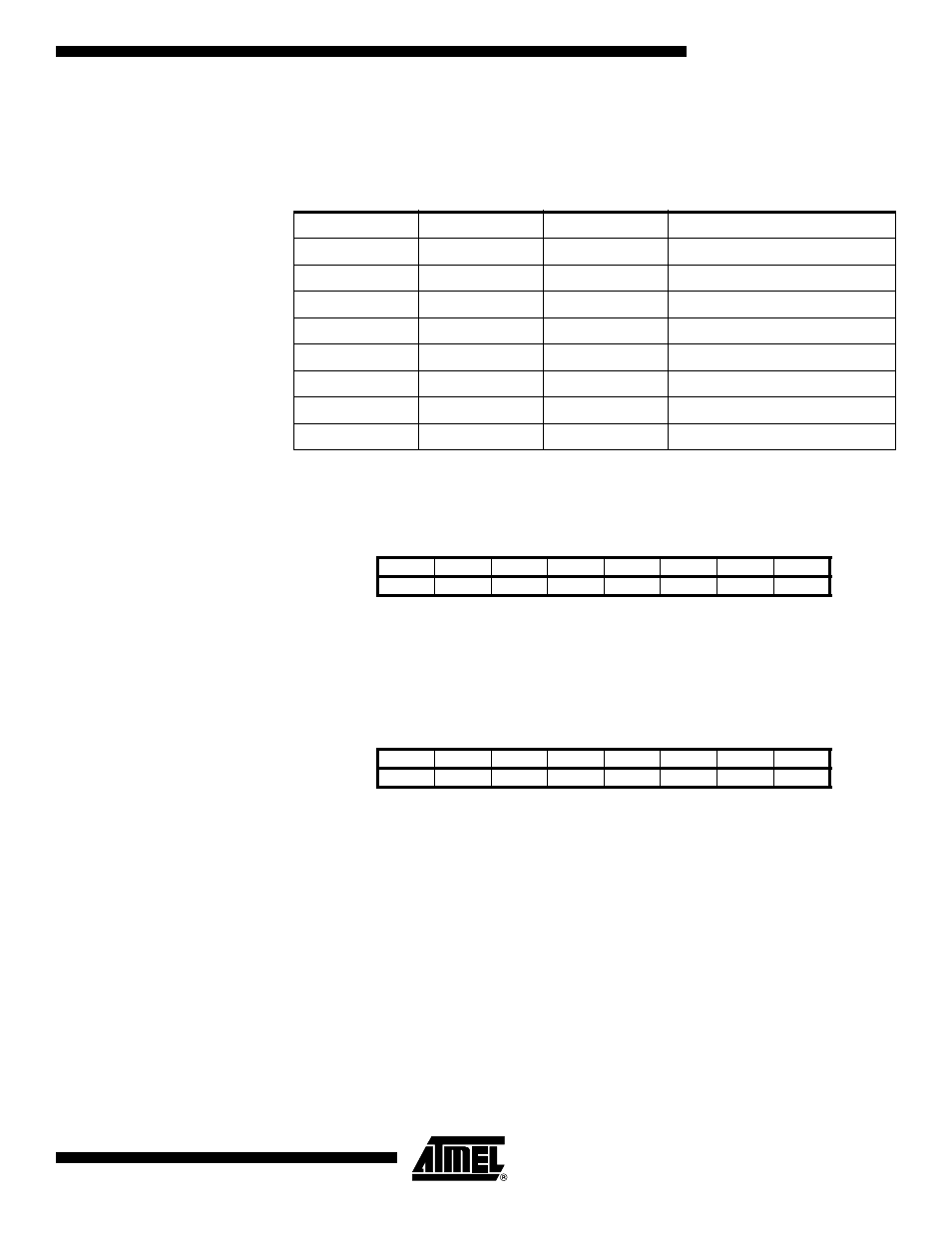
Table 91. ADC Prescaler Selections
ADPS2
ADPS1
ADPS0
Division Factor
0
0
0
2
0
0
1
2
0
1
0
4
0
1
1
8
1
0
0
16
1
0
1
32
1
1
0
64
1
1
1
128
Bit
15
14
13
12
11
10
9
8
–
–
–
–
–
–
ADC9
ADC8
ADCH
ADC7
ADC6
ADC5
ADC4
ADC3
ADC2
ADC1
ADC0
ADCL
7
6
5
4
3
2
1
0
Read/Write
R
R
R
R
R
R
R
R
R
R
R
R
R
R
R
R
Initial Value
0
0
0
0
0
0
0
0
0
0
0
0
0
0
0
0
Bit
15
14
13
12
11
10
9
8
ADC9
ADC8
ADC7
ADC6
ADC5
ADC4
ADC3
ADC2
ADCH
ADC1
ADC0
–
–
–
–
–
–
ADCL
7
6
5
4
3
2
1
0
Read/Write
R
R
R
R
R
R
R
R
R
R
R
R
R
R
R
R
Initial Value
0
0
0
0
0
0
0
0
0
0
0
0
0
0
0
0