Pin configurations, Disclaimer, Atmega169v/l – Rainbow Electronics Atmega169L User Manual
Page 2: Figure 1. pinout atmega169, Atmega169
2
ATmega169V/L
2514A–AVR–08/02
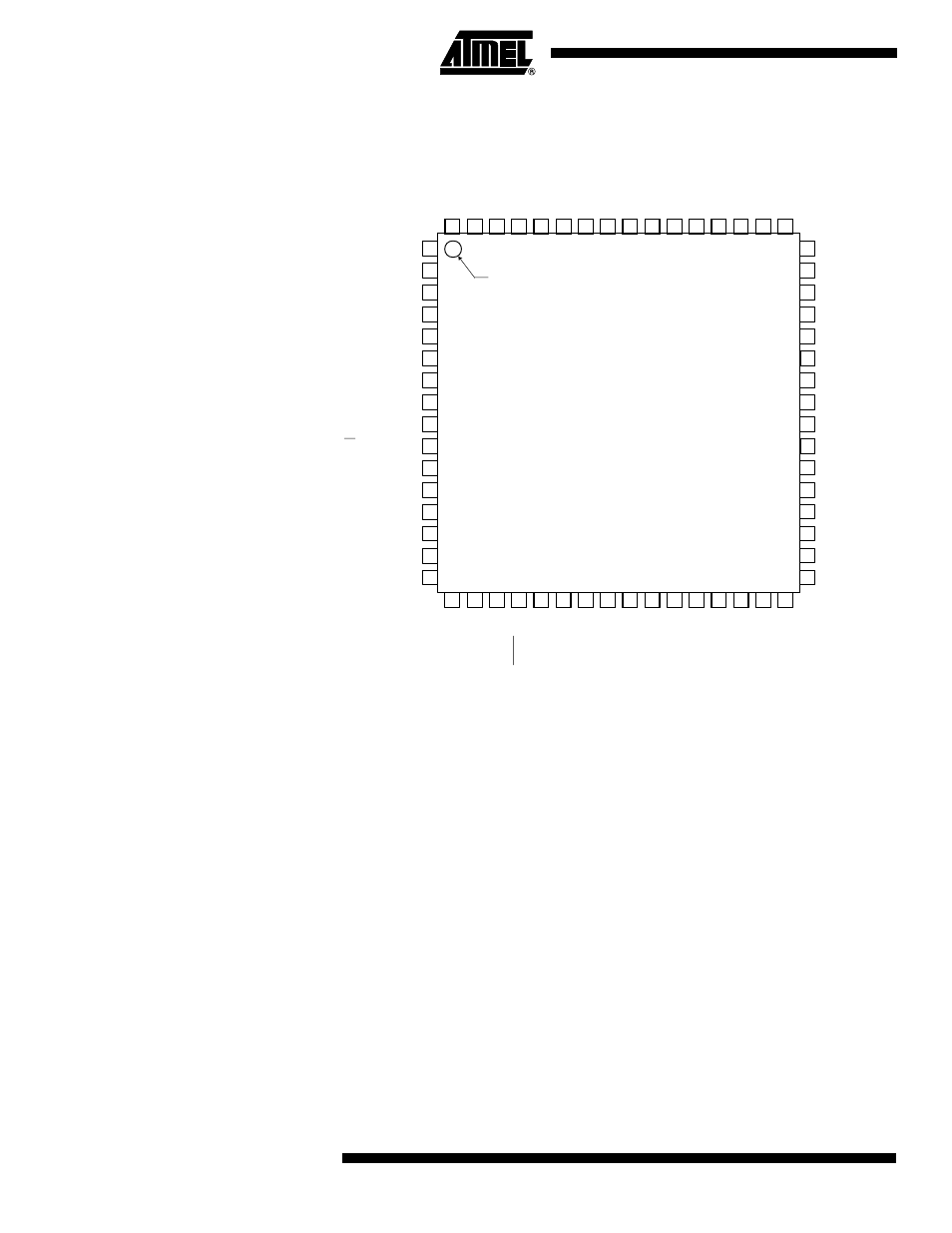
Pin Configurations
Figure 1. Pinout ATmega169
Disclaimer
Typical values contained in this data sheet are based on simulations and characteriza-
tion of other AVR microcontrollers manufactured on the same process technology. Min
and Max values will be available after the device is characterized.
PC0 (SEG12)
VCC
GND
PF0 (ADC0)
PF7 (ADC7/TDI)
PF1 (ADC1)
PF2 (ADC2)
PF3 (ADC3)
PF4 (ADC4/TCK)
PF5 (ADC5/TMS)
PF6 (ADC6/TDO)
AREF
GND
AVCC
17
61
60
18
59
20
58
19
21
57
22
56
23
55
24
54
25
53
26
52
27
51
29
28
50
49
32
31
30
(RXD/PCINT0) PE0
(TXD/PCINT1) PE1
LCDCAP
(XCK/AIN0/PCINT2) PE2
(AIN1/PCINT3) PE3
(USCK/SCL/PCINT4) PE4
(DI/SDA/PCINT5) PE5
(DO/PCINT6) PE6
(CLKO/PCINT7) PE7
(SS/PCINT8) PB0
(SCK/PCINT9) PB1
(MOSI/PCINT10) PB2
(MISO/PCINT11) PB3
(OC0A/PCINT12) PB4
(OC2A/PCINT15) PB7
(T1/SEG24) PG3
(OC1B/PCINT14) PB6
(T0/SEG23) PG4
(OC1A/PCINT13) PB5
PC1 (SEG11)
PG0 (SEG14)
(SEG15) PD7
PC2 (SEG10)
PC3 (SEG9)
PC4 (SEG8)
PC5 (SEG7)
PC6 (SEG6)
PC7 (SEG5)
PA7 (SEG3)
PG2 (SEG4)
PA6 (SEG2)
PA5 (SEG1)
PA4 (SEG0)
PA3 (COM3)
PA0 (COM0)
PA1 (COM1)
PA2 (COM2)
PG1 (SEG13)
(SEG16) PD6
(SEG17) PD5
(SEG18) PD4
(SEG19) PD3
(SEG20) PD2
(INT0/SEG21) PD1
(ICP/SEG22) PD0
(TOSC1) XTAL1
(TOSC2) XTAL2
(RESET) PG5
GND
VCC
ATmega169
INDEX CORNER
2
3
1
4
5
6
7
8
9
10
11
12
13
14
16
15
64
63
62
47
46
48
45
44
43
42
41
40
39
38
37
36
35
33
34