Timer 2 lsb (tl2), Timer 2 msb (th2), Clock output register (cor) – Maxim Integrated High-Speed Microcontroller Users Guide: Network Microcontroller Supplement User Manual
Page 74

High-Speed Microcontroller User’s
Guide: Network Microcontroller
Supplement
74
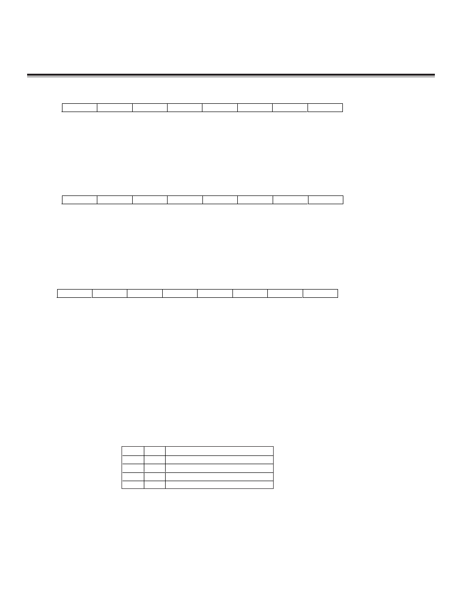
Timer 2 LSB (TL2)
R = Unrestricted read, W = Unrestricted write, -n = Value after reset
Timer 2 MSB (TH2)
R = Unrestricted read, W = Unrestricted write, -n = Value after reset
Clock Output Register (COR)
R = Unrestricted read, T = Timed-access write only, -n = Value after reset
7
6
5
4
3
2
1
0
SFR CCh
TL2.7
TL2.6
TL2.5
TL2.4
TL2.3
TL2.2
TL2.1
TL2.0
RW-0
RW-0
RW-0
RW-0
RW-0
RW-0
RW-0
RW-0
7
6
5
4
3
2
1
0
SFR CDh
TH2.7
TH2.6
TH2.5
TH2.4
TH2.3
TH2.2
TH2.1
TH2.0
RW-0
RW-0
RW-0
RW-0
RW-0
RW-0
RW-0
RW-0
7
6
5
4
3
2
1
0
SFR CEh
IRDACK
—
—
C0BPR7
C0BPR6
COD1
COD0
XCLKOE
RT-0
RT-1
RT-1
RT-0
RT-0
RT-0
RT-0
RT-0
TL2.7–0
Bits 7–0
Timer 2 LSB. This register contains the least significant byte of timer 2.
TH2.7–0
Bits 7–0
Timer 2 MSB. This register contains the most significant byte of timer 2.
XCLKOE
Bit 0
External clock output enable. XCLKOE = 1 enables a clock defined by COD1-COD0 and IRDACK to
be driven from the port pin P3.5. XCLKOE = 1 provides a full push-pull driver on P3.5. COD1 and COD0
are in “don’t care” states when XCLKOE and IRDACK are set to logic 1, causing the serial port baud
rate to be multiplied by 16. XCLKOE = 0 disables the clock output and leaves the P3.5 pin to function
as a general-purpose I/O port (GPIO) or as the T1 alternate function.
IRDACK
Bit 7
Bits 6-5
C0BPR7, C0BPR6
Bits 4-3
COD1, COD0
Bits 2-1
IRDA clock output enable. When XCLKOE = 0, IRDACK bit assumes a “don’t care” condition. When
XCLKOE = 1 and IRDACK = 1, the clock output pad issues a clock that is 16 times the baud rate of the
programmed baud rate associated with serial port 0. When XCLKOE = 1 and IRDACK = 0, the clock out-
put pad is controlled by the clock output divide select bits, COD1 and COD0. Note that the appropriate
baud rate must be established by use of timer 1 programmed for the baud-rate generator mode 2.
Reserved.
CAN 0 baud-rate prescaler bits. The C0BPR7 and C0BPR6 bits establish the two high-order bits asso-
ciated with the 8-bit baud-rate prescaler in the CAN 0 controller. Note that the C0BPR7 and C0BPR6 bits
cannot be written when the SWINT bit in the CAN 0 control register is cleared to 0. These bits do not
exist in the DS80C411.
Clock output divide select bits. The clock output divide bits are used to establish the output clock fre-
quency from the CLKO function on port pin P3.5, when enabled by the COR.0 (XCLKOE) bit. Consult
the description of the XCLKOE bit for more information.
COD1
COD0
P3.5 OUTPUT FREQUENCY
0
0
System clock divided by 2
0
1
System clock divided by 4
1
0
System clock divided by 6
1
1
System clock divided by 8
Maxim Integrated
