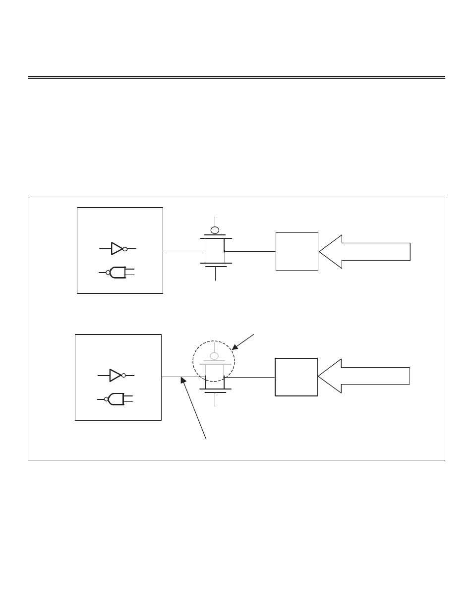
5v-tolerant i/o, 3v internal logic (v, 3v) pad i/o 3.3v input pad i/o 5v input – Maxim Integrated High-Speed Microcontroller Users Guide: Network Microcontroller Supplement User Manual
Page 117: Internal logic (v, 3v) v

5V-Tolerant I/O
In order for the DS80C400 to provide 5V-tolerant I/O, additional circuitry has been incorporated to detect I/O pad voltages that exceed
V
CC3
. When these levels are detected, the circuitry enables protective switching to prevent undesirable voltages from reaching inter-
nal V
CC3
logic. During the protective switching process, the pin sinks additional current, not to exceed 100µA, to V
CC3.
I/O signals with
long rise or fall times spend more time transitioning through the protective switching process drawing more current and should be
avoided in 5V-tolerant mode. Steady state voltages on I/O between (V
CC3
+ 0.3V) and (V
CC3
+ 0.7V) draw excessive current in 5V-tol-
erant mode. When the switch completes, the external pad input is required to source ~2µA in order to sustain the internal switching
circuit. Following the protective switch, the pad input cannot drive the internal logic nodes completely to V
CC3
, therefore resulting in
some additional static V
CC3
current draw. The amount of additional current depends upon factors that include I/O pad voltage, V
CC3
voltage, and temperature, but again should not exceed 100µA per pin and typically is in the ~1-10µA range. If the I/O is limited to the
V
CC3
supply range, these additional currents are not present. A simplified depiction of the 5V-tolerant I/O protection scheme is shown
in Figure 10-1.
Figure 10-1. 5V-Tolerant I/O Pad
High-Speed Microcontroller User’s
Guide: Network Microcontroller
Supplement
117
V
CC3
= 3.3V
INTERNAL LOGIC
(V
CC3
= 3.3V)
PAD
I/O
3.3V INPUT
PAD
I/O
5V INPUT
Pch device of transmission
gate gets switched off.
Internal voltage = V
CC3
- V
T
(Nch device)
INTERNAL LOGIC
(V
CC3
= 3.3V)
V
CC3
= 3.3V
Maxim Integrated
