Byte masks, Sdram register descriptions, Sdram control register (sdconf) – Cirrus Logic EP73xx User Manual
Page 83: Byte masks -3, Sdram register descriptions -3, Sdram control register (sdconf) -3
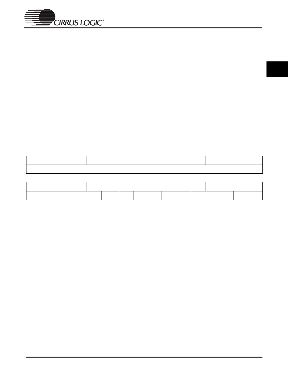
EP7309/11/12 User’s Manual - DS508UM4
7-3
Copyright Cirrus Logic, Inc. 2003
SDRAM Controller
77
7
The SDRAM controller will continue to provide refresh cycles at the rate set in
SDRFPR until the SDACTIVE bit is set to 0 or the CPU is reset.
Byte Masks
Pins
PD6
and
PD7
are multiplexed with the
SDQM0
and
SDQM1
signals, respectively.
ENPD67, bit 10 in the SYSCON3 register, enables pins
PD6
and
PD7
as GPIO bits
when set. This is useful in applications which do not involve the SDRAM interface.
When cleared, pins
PD6
and
PD7
represent the
SDQM0
and
SDQM1
output signals
from the SDRAM controller. ENPD67 must be cleared in order to properly use the
SDRAM interface.
SDRAM Register Descriptions
SDRAM Control Register (SDCONF)
Address:
0x8000.2300, Read / Write
Definition:
SDRAM Configuration Data Register.
Bit Descriptions:
RSVD:
Reserved. Unknown during read.
CASLAT[1:0]: Number of clock cycles after CAS before the device is ready for
reading or writing:
00 = reserved
01 = reserved
10 = CAS latency = 2
11 = CAS latency = 3
The default value is ‘10’ for CAS latency = 2.
SDSIZE[1:0]: Indicates the capacity of each SDRAM device:
00 = 16 Mbit
01 = 64 Mbit
10 = 128 Mbit
11 = 256 Mbit
31
30
29
28
27
26
25
24
23
22
21
20
19
18
17
16
RSVD
15
14
13
12
11
10
9
8
7
6
5
4
3
2
1
0
RSVD
SDACTIVE
CLKCTL
SDWIDTH[1:0]
SDSIZE[1:0]
RSVD
CASLAT[1:0]