External signal functions, Table 1-4: external signal functions -7 – Cirrus Logic EP73xx User Manual
Page 21
EP7309/11/12 User’s Manual - DS508UM4
1-7
Copyright Cirrus Logic, Inc. 2003
Introduction
11
1
External Signal Functions
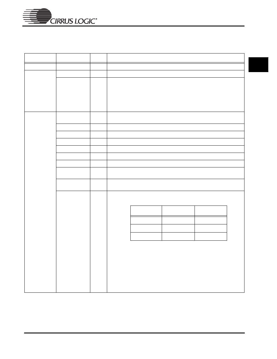
Table 1-4: External Signal Functions
Function
Signal Name
Signal
Description
Data bus
D[0-31]
I/O
32-bit system data bus for memory, SDRAM, and I/O interface
Address bus
A[0-31]
O
32 bits of system byte address during memory and expansion cycles
A[27-13]/
DRA[0-14]
O
DRA[0-14] are multiplexed with A[27-13] for SDRAM memory accesses. A27
corresponds to DRA0 on SDRAM device. This offers additional power savings since
the lightest loading is expected on the high order ROM address lines.
Whenever the EP73xx is in the Standby State, the external address and data buses
are driven low. The RUN signal is used internally to force these buses to be driven
low. This is done to prevent peripherals that are powered-down from draining current.
Also, the internal peripheral’s signals get set to their Reset State.
Memory Interface
BA[0-1]/
A[13-14]
I/O
A13 and A14, during SDRAM accesses, become bank select pins BA0 and BA1.
nMOE/nSDCAS
O
ROM expansion OP enable/ SDRAM CAS control signal
nMWE/nSDWE
O
ROM expansion write enable/ SDRAM write enable control signal
nCS[0-5]
O
Chip select; active low, SRAM-like chip selects for expansion
SDQM[0-1]
O
LDQM; lower byte masks for SDRAM accesses
SDQM[2-3]
O
UDQM; upper byte masks for SDRAM/ multiplexed with PD[6-7]. See GPIO section
SDCS[0-1]
O
SDRAM chip selects
EXPRDY
I
Expansion port ready; external expansion devices drive this low to extend the bus
cycle. This is used to insert wait states for an external bus cycle.
WRITE/nSDRAS
O
Transfer Direction for expansion bus/SDRAM RAS control signal during SDRAM
access
WORD/
HALFWORD
O
To do write accesses of different sizes Word and Half-Word must be externally
decoded. The encoding of these signals is as follows:
The core will generate an address. When doing a read, the ARM core will select the
appropriate byte channels. When doing a write, the correct bytes will have to be
enabled depending on the above signals and the least significant bits of the address
bus.
The ARM architecture does not support unaligned accesses. For a read using x 32
memory, it is assumed that you will ignore bits 1 and 0 of the address bus and
perform a word read (or in power critical systems decode the relevant bits depending
on the size of the access). If an unaligned read takes place, the core will rotate the
resulting data in the register. For more information on this behavior see the LDR
instruction in the ARM7TDMI data sheet.
Access Size
Word
Half-Word
Word
1
0
Half-Word
0
1
Byte
0
0