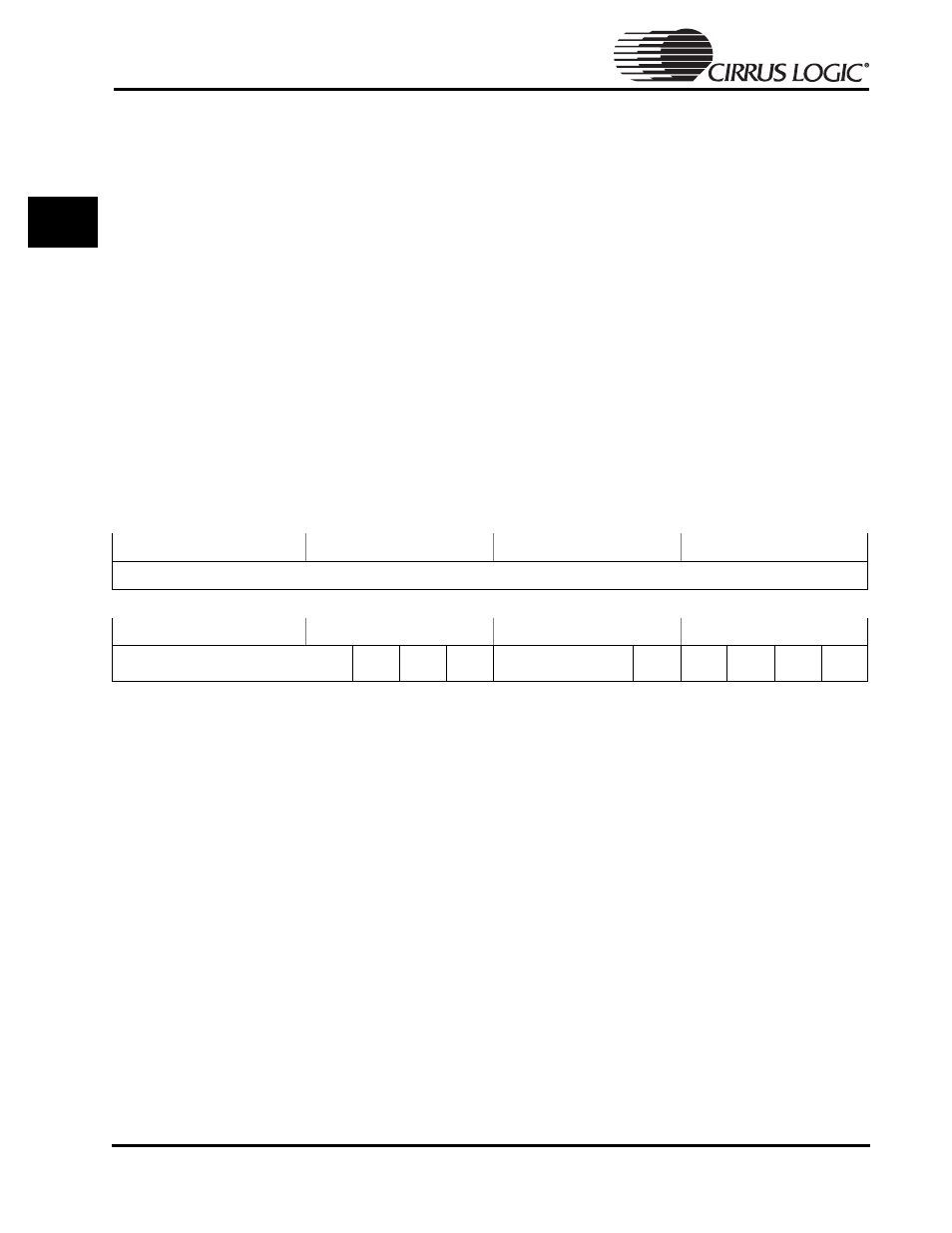
System control register 3 (syscon3), System control register 3 (syscon3) -8, Select. when low, the – Cirrus Logic EP73xx User Manual
Page 68: Signal will be output on the, Pin. when high, the, Signal will be output on, Buzfreq: selects the hardware source for the

5-8
EP7309/11/12 User’s Manual - DS508UM4
Copyright Cirrus Logic, Inc. 2003
System Registers
5
SS2MAEN: Master mode enable for the synchronous serial interface 2. When
low, SSI2 will be configured for slave mode operation. When high,
SSI2 will be configured for master mode operation. This bit also
controls the directionality of the interface pins.
OSTB:
This bit (operating system timing bit) is for use only with the
13 MHz clock source mode. Normally it will be set low, however
when set high it will cause a 500 kHz clock to be generated for the
timers instead of the 541 kHz which would normally be available.
The divider to generate this frequency is not clocked when this bit
is set low.
CLKENSL:
CLKEN
select. When low, the
CLKEN
signal will be output on the
RUN
/
CLKEN
pin. When high, the
RUN
signal will be output on
RUN
/
CLKEN
.
BUZFREQ: Selects the hardware source for the
BUZ
pin. When set, a fixed
500 Hz (528 Hz in 13 MHz mode and 612 Hz at 90 MHz) clock is
used as the source. When cleared, the overflow bit from timer TC1
is used as the clock signal.
System Control Register 3 (SYSCON3)
Address:
0x8000.2200, Read / Write
Definition:
The SYSCON3 system control register is a 11-bit read/write register
which controls some of the general configuration parameters for the
EP73xx as well as the control and status of internal peripherals. All
bits in this register are cleared upon system reset (nSYSRES).
Bit Descriptions:
ADCCON: Determines whether the ADC Configuration Extension field
SYNCIO[16-31] is to be used for ADC configuration data. When
this bit = 0 (default state) the ADC Configuration Byte SYNCIO[0-
7] only is used for backwards compatibility. When this bit = 1, the
ADC Configuration Extension field in the SYNCIO register is
used for ADC Configuration data and the value in the ADC
Configuration Byte (SYNCIO[0-6]) selects the length of the data
(8-bit to 16-bit).
CLKCTL:
This two-bit field determines the clock speed for the ARM720T
core, the clock speed for the memory bus, and the wait state
scaling factor. When operating the CPU from an external 13 MHz
clock, CLKCTL must be set to 00. The following table lists the
options.
31
30
29
28
27
26
25
24
23
22
21
20
19
18
17
16
RSVD
15
14
13
12
11
10
9
8
7
6
5
4
3
2
1
0
RSVD
ENPD67
128Fs
Reserve
d-0
VERSN (read-only)
ADCCK
NSEN
DAISEL
CLKCTL
1
CLKCTL
0
ADCCO
N
