Cirrus Logic EP73xx User Manual
Page 23
EP7309/11/12 User’s Manual - DS508UM4
1-9
Copyright Cirrus Logic, Inc. 2003
Introduction
11
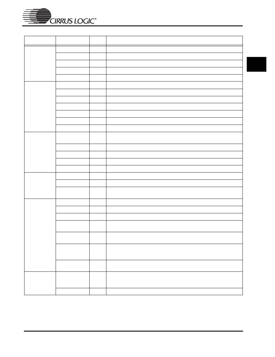
1
ADC
Interface
(SSI1)
ADCCLK
O
Serial clock output
nADCCS
O
Chip select for ADC interface
ADCOUT
O
Serial data output
ADCIN
I
Serial data input
SMPCLK
O
Sample clock output
IrDA and
RS232
Interfaces
LEDDRV
O
Infrared LED drive output (UART1)
PHDIN
I
Photo diode input (UART1)
TXD[1-2]
O
RS232 UART1 and 2 TX outputs
RXD[1-2]
I
RS232 UART1 and 2 RX inputs
DSR
I
RS232 DSR input
DCD
I
RS232 DCD input
CTS
I
RS232 CTS input
LCD
DD[0-3]
I/O
LCD serial display data; pins can be used on power up to read the ID of some LCD
modules (See
).
CL[1]
O
LCD line clock
CL[2]
O
LCD pixel clock
FRM
O
LCD frame synchronization pulse output
M
O
LCD AC bias drive
Keyboard &
Buzzer drive
LED Flasher
COL[0-7]
O
Keyboard column drives (SYSCON1)
BUZ
O
Buzzer drive output (SYSCON1)
PD[0]/
LEDFLSH
O
LED flasher driver — multiplexed with Port D bit 0. This pin can provide up to 4 mA
of drive current.
General
Purpose I/O
PA[0-7]
I/O
Port A I/O (bit 6 for boot clock option); also used as keyboard row inputs
PB[0-7]
I/O
Port B I/O. All eight Port B bits can be used as GPIOs.
PD[0-5]
I/O
Port D I/O / PD0 multiplexed at LEDFLSH. See above.
PD[6-7]/SDQM
[0-1]
I/O
Port D I/O/dedicated byte mask select for SDRAM
PE[0]/
BOOTSEL[0]
I/O
Port E I/O (3 bits only). Can be used as general purpose I/O during normal
operation.
PE[1]/
BOOTSEL[1]
I/O
During power-on reset, PE[0] and PE[1] are inputs and are latched by the rising edge
of nPOR to select the memory width that the EP73xx will use to read from the boot
code storage device (i.e., external 8-bit-wide FLASH bank).
PE[2]/
CLKSEL
I/O
During power-on reset, PE[2] is latched by the rising edge of nPOR to select the
clock mode of operation (i.e., either the PLL or external 13 MHz clock mode).
PWM
Drives
DRIVE[0-1]
I/O
PWM drive outputs. These pins are inputs on power up to determine what polarity
the output of the PWM should be when active. Otherwise, these pins are always an
output (See
).
FB[0-1]
I
PWM feedback inputs
Table 1-4: External Signal Functions (Continued)
Function
Signal Name
Signal
Description