Table 6-3: memory map in external boot mode -3 – Cirrus Logic EP73xx User Manual
Page 77
EP7309/11/12 User’s Manual - DS508UM4
6-3
Copyright Cirrus Logic, Inc. 2003
Processor Support
66
6
External ROM i.e., FLASH or EEPROM will be configured for access by
CS0
and the
processor will begin fetching instructions from address 0x0. Before this will occur, the
processor must be put into operating state as described in the power-up sequence.
The default memory map before the MMU is enabled and configured is as seen
below. Note that any of the chip selects can be reconfigured once the processor is in
operating state and properly fetching instructions.
CS0
by default will access memory
with the maximum number of wait states for either random or sequential accesses
which will require re-programming of the MEMCFG1 register to optimize
performance for ROM accesses.
Note: For configuration of the individual chip selects, refer to the SDRAM/SRAM
chapter of the manual for full details.
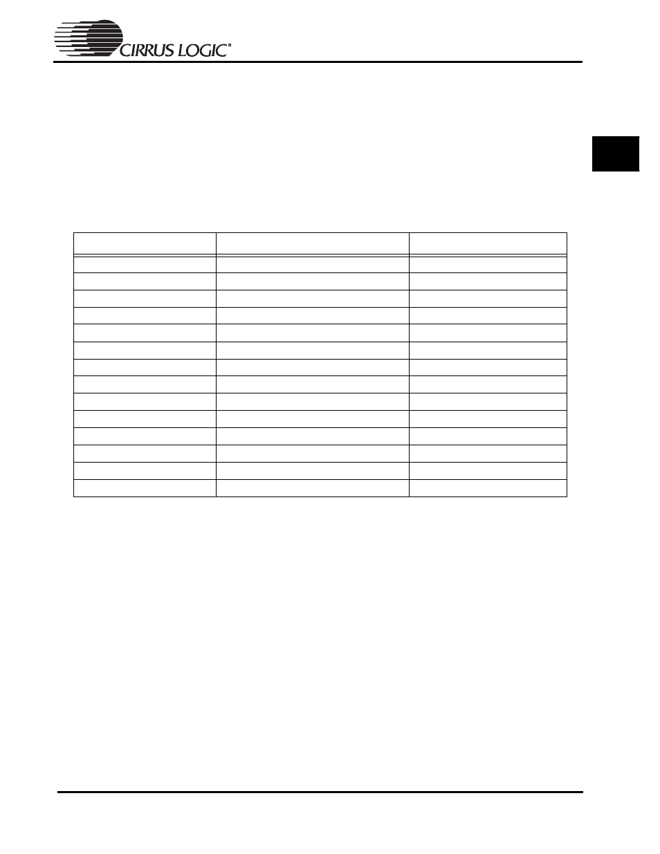
Table 6-3: Memory Map in External Boot Mode
Address
Contents
Size
0xF000.0000
Reserved
256 Mbytes
0xE000.0000
Reserved
256 Mbytes
0xD000.0000
Reserved
256 Mbytes
0xC000.0000
SDRAM
64 Mbytes
0x8000.4000
Unused
~1 Gbyte
0x8000.0000
Internal registers
16 Kbytes
0x7000.0000
Boot ROM (nCS[7])
128 bytes
0x6000.0000
SRAM (nCS[6])
48,400 bytes
0x5000.0000
Expansion (nCS[5])
256 Mbytes
0x4000.0000
Expansion (nCS[4])
256 Mbytes
0x3000.0000
Expansion (nCS[3])
256 Mbytes
0x2000.0000
Expansion (nCS[2])
256 Mbytes
0x1000.0000
ROM Bank 1 (nCS[1])
256 Mbytes
0x0000.0000
ROM Bank 0 (nCS[0])
256 Mbytes