Cirrus Logic EP73xx User Manual
Page 18
1-4
EP7309/11/12 User’s Manual - DS508UM4
Copyright Cirrus Logic, Inc. 2003
Introduction
1
Note: All byte-wide registers should be accessed as words (except Port A to Port D
registers, which are designed to work in both word and byte modes).
All registers bit alignment starts from the LSB of the register (i.e., they are all
right shift justified). The registers which interact with the 32 kHz clock or which
could change during readback (i.e., RTC data registers, SYSFLG1 register
(lower 6-bits only), the TC1D and TC2D data registers, port registers, and
interrupt status registers), should be read twice and compared to ensure that a
stable value has been read back.
All internal registers in the EP73xx are reset (cleared to zero) by a system reset (i.e.,
nPOR
,
nRESET
, or
nPWRFL
signals becoming active), and the Real Time Clock data
register (RTCDR) and match register (RTCMR), which are only reset by
nPOR
becoming active. This ensures that the system time preserved through a user reset or
power fail condition. In the following register descriptions, little endian is assumed.
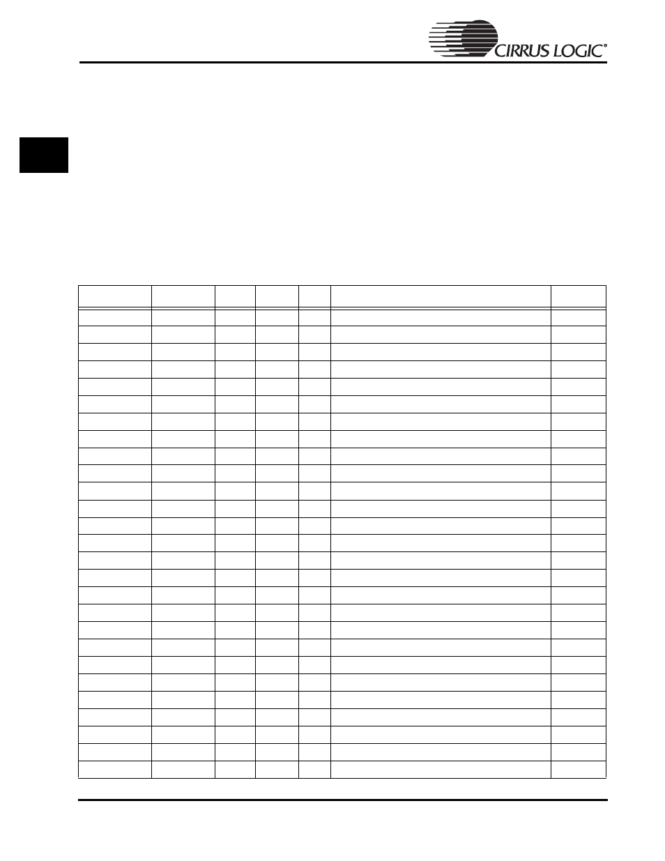
Table 1-2: EP73xx Internal Registers (Little Endian Mode)
Address
Name
Default RD/WR
Size
Comments
Page
0x8000.0000
PADR
0
RW
8
Port A data register
0x8000.0001
PBDR
0
RW
8
Port B data register
0x8000.0002
—
—
8
Reserved
0x8000.0003
PDDR
0
RW
8
Port D data register
0x8000.0040
PADDR
0
RW
8
Port A data direction register
0x8000.0041
PBDDR
0
RW
8
Port B data direction register
0x8000.0042
—
—
8
Reserved
0x8000.0043
PDDDR
0
RW
8
Port D data direction register
0x8000.0080
PEDR
0
RW
3
Port E data register
0x8000.00C0
PEDDR
0
RW
3
Port E data direction register
0x8000.0100
SYSCON1
0
RW
32
System control register 1
0x8000.0140
SYSFLG1
0
RD
32
System status flags register 1
0x8000.0180
MEMCFG1
0
RW
32
Expansion memory configuration register 1
0x8000.01C0
MEMCFG2
0
RW
32
Expansion memory configuration register 2
0x8000.0200
0
RW
32
Reserved
0x8000.0240
INTSR1
0
RD
32
Interrupt status register 1
0x8000.0280
INTMR1
0
RW
32
Interrupt mask register 1
0x8000.02C0
LCDCON
0
RW
32
LCD control register
0x8000.0300
TC1D
0
RW
16
Read / Write register sets and reads data to TC1
0x8000.0340
TC2D
0
RW
16
Read / Write register sets and reads data to TC2
0x8000.0380
RTCDR
—
RW
32
Real Time Clock data register
0x8000.03C0
RTCMR
—
RW
32
Real Time Clock match register
0x8000.0400
PMPCON
0
RW
12
PWM pump control register
0x8000.0440
CODR
0
RW
8
CODEC data I/O register
0x8000.0480
UARTDR1
0
RW
16
UART1 FIFO data register
0x8000.04C0
UBRLCR1
0
RW
32
UART1 bit rate and line control register
0x8000.0500
SYNCIO
0
RW
32
Synchronous serial I/O data register for master only SSI