I2c ac electrical characteri, Nonvolatile memory character, C ac electrical characteristics – Rainbow Electronics DS1874 User Manual
Page 8: Nonvolatile memory characteristics, Ds1874 sfp+ controller with digital ldd interface
Note 1:
All voltages are referenced to ground. Current into the IC is positive, and current out of the IC is negative.
Note 2:
Inputs are at supply rail. Outputs are not loaded.
Note 3:
This parameter is guaranteed by design.
Note 4:
Full-scale is user programmable.
Note 5:
The DACs are the bias and modulation DACs found in the MAX3798/MAX3799 that are controlled by the DS1874.
Note 6:
The DS1874 is configured with TXDOUT connected to the MAX3798/MAX3799 DISABLE input.
Note 7:
This includes writing to the modulation DAC and the initial step written to the bias DAC.
Note 8:
A temperature conversion is completed and the modulation register value is recalled from the LUT and V
CC
has been
measured to be above V
CC
LO alarm.
Note 9:
The timing is determined by the choice of the update rate setting (see Table 02h, Register 88h).
Note 10: This specification is the time it takes from MON3 voltage falling below the LLOS trip threshold to LOSOUT asserted high.
Note 11: This specification is the time it takes from MON3 voltage rising above the HLOS trip threshold to LOSOUT asserted low.
Note 12: Assuming an appropriate initial step is programmed that would cause the power to exceed the APC set point within four
steps, the bias current will be within 3% within the time specified by the binary search time. See the
BIAS and MODULA-
TION Control During Power-Up section.
Note 13: I
2
C interface timing shown is for fast mode (400kHz). This device is also backward compatible with I
2
C standard mode
timing.
Note 14: C
B
—the total capacitance of one bus line in pF.
Note 15: EEPROM write begins after a STOP condition occurs.
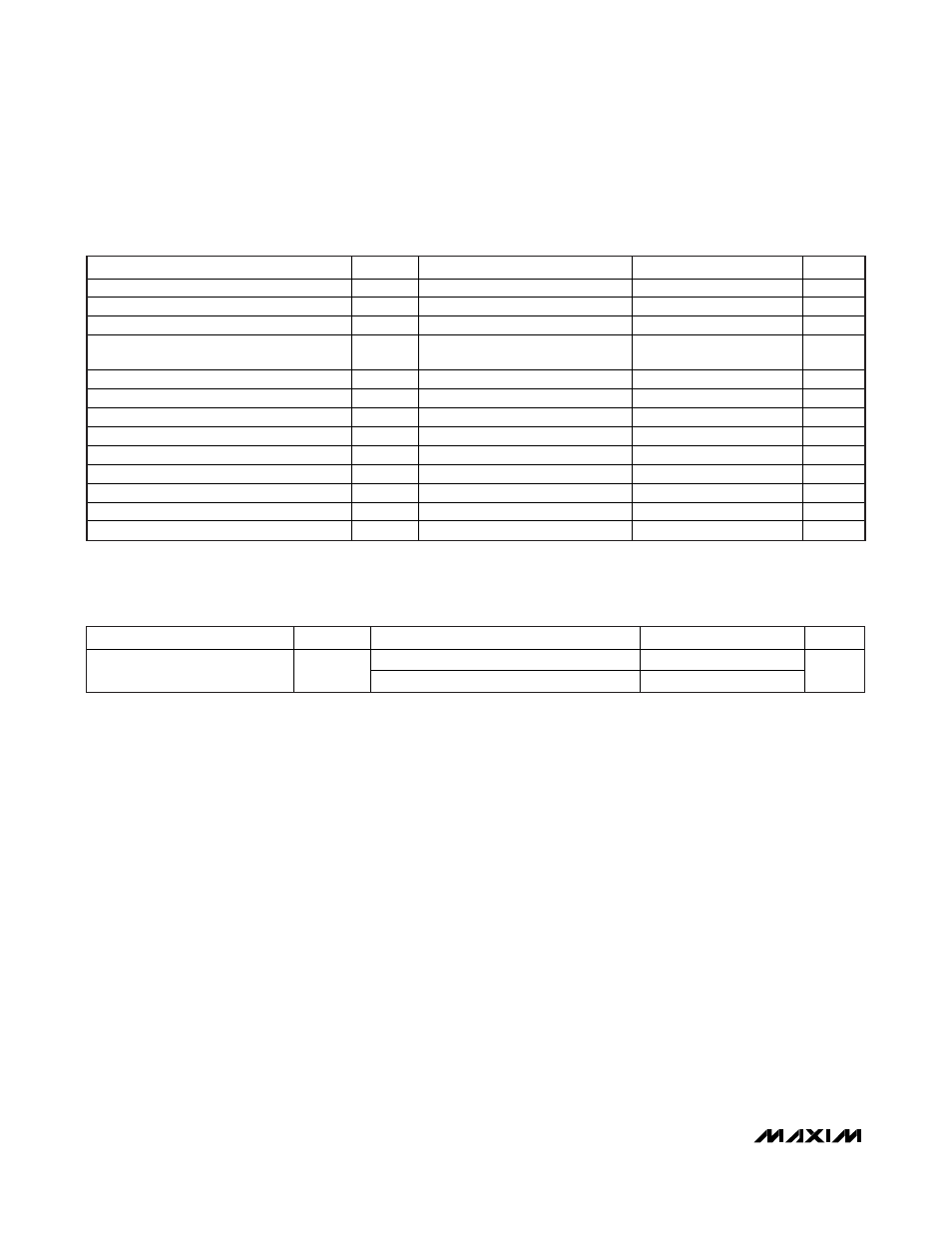
PARAMETER
SYMBOL
CONDITIONS
MIN
TYP
MAX
UNITS
SCL Clock Frequency
f
SCL
(Note
13)
0
400 kHz
Clock Pulse-Width Low
t
LOW
1.3
μs
Clock Pulse-Width High
t
HIGH
0.6
μs
Bus-Free Time Between STOP and START
Condition
t
BUF
1.3
μs
START Hold Time
t
HD:STA
0.6
μs
START Setup Time
t
SU:STA
0.6
μs
Data Out Hold Time
t
HD:DAT
0
0.9
μs
Data In Setup Time
t
SU:DAT
100
ns
Rise Time of Both SDA and SCL Signals
t
R
(Note 14)
20 + 0.1C
B
300
ns
Fall Time of Both SDA and SCL Signals
t
F
(Note 14)
20 + 0.1C
B
300
ns
STOP Setup Time
t
SU:STO
0.6
μs
EEPROM Write Time
t
W
(Note
15)
20 ms
Capacitive Load for Each Bus Line
C
B
400 pF
DS1874
SFP+ Controller with Digital LDD Interface
8
_______________________________________________________________________________________
NONVOLATILE MEMORY CHARACTERISTICS
(V
CC
= +2.85V to +3.9V, unless otherwise noted.)
PARAMETER
SYMBOL
CONDITIONS
MIN
TYP
MAX
UNITS
At +25°C
200,000
EEPROM Write Cycles
At +85°C
50,000
I
2
C AC ELECTRICAL CHARACTERISTICS
(V
CC
= +2.85V to +3.9V, T
A
= -40°C to +95°C, timing referenced to V
IL(MAX)
and V
IH(MIN)
, unless otherwise noted. See Figure 17.)