Ds1874 sfp+ controller with digital ldd interface – Rainbow Electronics DS1874 User Manual
Page 60
DS1874
SFP+ Controller with Digital LDD Interface
60
______________________________________________________________________________________
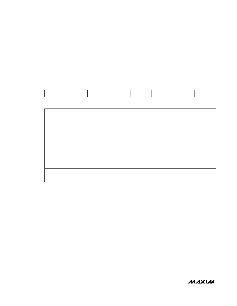
Table 02h, Register 8Ah: CNFGB
FACTORY
DEFAULT
00h
READ ACCESS
PW2 or (PW1 and RWTBL246) or (PW1 and RTBL246)
WRITE ACCESS
PW2 or (PW1 and RWTBL246)
MEMORY
TYPE Nonvolatile
(SEE)
8Ah
IN1C
INVOUT1 RESERVED RESERVED RESERVED ALATCH QTLATCH WLATCH
BIT
7
BIT
0
BIT
7
IN1C: IN1 Software Control Bit (see Figure 13).
0 = IN1 pin’s logic controls OUT1 pin.
1 = OUT1 is active (bit 6 defines the polarity).
BIT
6
INVOUT1: Inverts the active state for OUT1 (see Figure 13).
0 = Noninverted.
1 = Inverted.
BITS
5:3 RESERVED
BIT
2
ALATCH: ADC Alarm’s Comparison Latch. Table 01h, Registers 70h–71h.
0 = ADC alarm flags reflect the status of the last comparison.
1 = ADC alarm flags remain set.
BIT
1
QTLATCH: Quick Trip’s Comparison Latch. Table 01h, Registers 72h–73h and 76h.
0 = QT alarm flags reflect the status of the last comparison.
1 = QT alarm flags remain set.
BIT
0
WLATCH: ADC Warning’s Comparison Latch. Table 01h, Registers 74h–75h.
0 = ADC warning flags reflect the status of the last comparison.
1 = ADC warning flags remain set.