Typical operating circuit, Detailed description, Max3798/max3799 dac control – Rainbow Electronics DS1874 User Manual
Page 12: Bias register/apc control, Ds1874 sfp+ controller with digital ldd interface
LOS
TXF
TXD
TXDOUT
RSEL
FAULT
DISABLE
RSEL
RSELOUT
LOS
LOSOUT
TX_FAULT
SDA
SCL
MODE_DEF2 (SDA)
RATE SELECT
LOS
MODE_DEF1 (SCL)
TX_DISABLE
MODE
DAC
BIAS
DAC
LDD
EEPROM
QUICK
TRIP
LOS
ADC
I
2
C
3W
3W
DS1874
MAX3798/MAX3799
MON1
MON2
MON3
BMON
R
MON
100
Ω
+3.3V
R
BD
LA
PIN-ROSA
VCSEL-TOSA
DS1874
SFP+ Controller with Digital LDD Interface
12
______________________________________________________________________________________
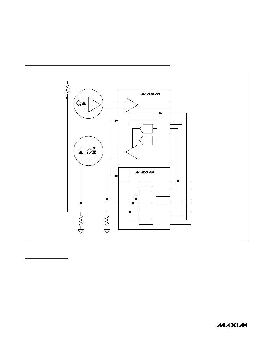
Detailed Description
The DS1874 integrates the control and monitoring func-
tionality required to implement a VCSEL-based SFP or
SFP+ system using Maxim’s MAX3798/MAX3799 com-
bined limiting amplifier and laser driver. Key compo-
nents of the DS1874 are shown in the
Block Diagram
and described in subsequent sections.
MAX3798/MAX3799 DAC Control
The DS1874 controls two 9-bit DACs inside the
MAX3798/MAX3799. One DAC is used for laser bias
control while the other is used for laser modulation con-
trol. The DS1874 communicates with the MAX3798/
MAX3799 over a 3-wire digital interface (see the
3-Wire
Master for Controlling the MAX3798/MAX3799
section).
The communication between the DS1874 and
MAX3798/MAX3799 is transparent to the end user.
BIAS Register/APC Control
The MAX3798/MAX3799 control their laser bias current
DAC using the APC loop within the DS1874. The APC
loop’s feedback to the DS1874 is the monitor diode
(MON2) current, which is converted to a voltage using
Typical Operating Circuit