Ds1874 sfp+ controller with digital ldd interface – Rainbow Electronics DS1874 User Manual
Page 59
DS1874
SFP+ Controller with Digital LDD Interface
______________________________________________________________________________________
59
FACTORY
DEFAULT
80h
READ ACCESS
PW2 or (PW1 and RWTBL246) or (PW1 and RTBL246)
WRITE ACCESS
PW2 or (PW1 and RWTBL246)
MEMORY TYPE
Nonvolatile (SEE)
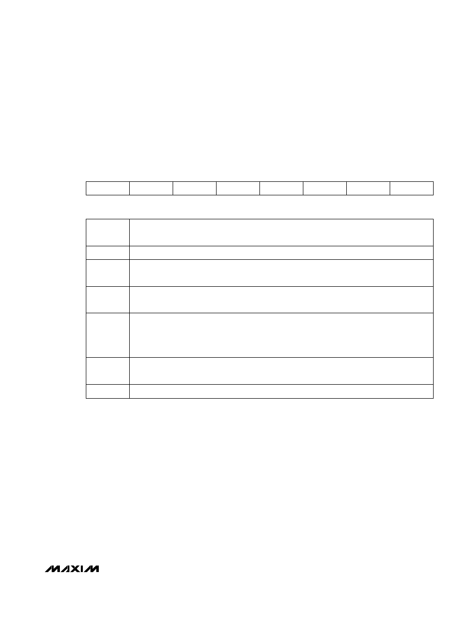
89h LOSC RESERVED INV
LOS
ASEL
MASK INVRSOUT
RESERVED
RESERVED
BIT
7
BIT
0
BIT
7
LOSC: LOS Configuration. Defines the source for the LOSOUT pin (see Figure 13).
0 = LOS LO alarm is used as the source.
1 = (Default) LOS input pin is used as the source.
BIT
6
RESERVED
BIT
5
INV LOS: Inverts the buffered input pin LOS to output pin LOSOUT (see Figure 13).
0 = Noninverted LOS to LOSOUT pin.
1 = Inverted LOS to LOSOUT pin.
BIT
4
ASEL: Address Select.
0 = Device address is A2h.
1 = Byte DEVICE ADDRESS in Table 02h, Register 8Ch is used as the device address.
BIT
3
MASK:
0 = Alarm-enable row exists at Table 01h, Registers F8h–FFh. Table 05h, Registers F8h–FFh are
empty.
1 = Alarm-enable row exists at Table 05h, Registers F8h–FFh. Table 01h, Registers F8h–FFh are
empty.
BIT
2
INVRSOUT: Allow for inversion of RSELOUT pin (see Figure 13).
0 = RSELOUT is not inverted.
1 = RSELOUT is inverted.
BITS
1:0
RESERVED
Table 02h, Register 89h: CNFGA